JAJSKH9C March   2012  – January 2021 INA282-Q1 , INA283-Q1 , INA284-Q1 , INA285-Q1 , INA286-Q1

PRODUCTION DATA  

  1. 特長
  2. アプリケーション
  3. 概要
  4. Revision History
  5. Pin Configuration and Functions
  6. Specifications
    1. 6.1 Absolute Maximum Ratings
    2. 6.2 ESD Ratings
    3. 6.3 Recommended Operating Conditions
    4. 6.4 Thermal Information
    5. 6.5 Electrical Characteristics
    6. 6.6 Typical Characteristics
  7. Detailed Description
    1. 7.1 Overview
    2. 7.2 Functional Block Diagram
    3. 7.3 Feature Description
      1. 7.3.1 Selecting RS
      2. 7.3.2 Effective Bandwidth
      3. 7.3.3 Transient Protection
    4. 7.4 Device Functional Modes
      1. 7.4.1 Reference Pin Connection Options
        1. 7.4.1.1 Unidirectional Operation
          1. 7.4.1.1.1 Ground Referenced Output
          2. 7.4.1.1.2 V+ Referenced Output
        2. 7.4.1.2 Bidirectional Operation
          1. 7.4.1.2.1 External Reference Output
          2. 7.4.1.2.2 Splitting the Supply
          3. 7.4.1.2.3 Splitting an External Reference
      2. 7.4.2 Shutdown
      3. 7.4.3 Extended Negative Common-Mode Range
      4. 7.4.4 Calculating Total Error
        1. 7.4.4.1 Example 1 INA282-Q1
        2. 7.4.4.2 Example 2 INA286-Q1
  8. Application and Implementation
    1. 8.1 Application Information
      1. 8.1.1 Basic Connections
    2. 8.2 Typical Applications
      1. 8.2.1 Current Summing
        1. 8.2.1.1 Design Requirements
        2. 8.2.1.2 Detailed Design Procedures
        3. 8.2.1.3 Application Curve
      2. 8.2.2 Current Differencing
        1. 8.2.2.1 Design Requirements
        2. 8.2.2.2 Detailed Design Procedure
        3. 8.2.2.3 Application Curve
  9. Power Supply Recommendations
  10. 10Layout
    1. 10.1 Layout Guidelines
    2. 10.2 Layout Example
  11. 11Device and Documentation Support
    1. 11.1 ドキュメントの更新通知を受け取る方法
    2. 11.2 サポート・リソース
    3. 11.3 Trademarks
    4. 11.4 静電気放電に関する注意事項
  12. 12用語集
  13. 13Mechanical, Packaging, and Orderable Information

パッケージ・オプション

メカニカル・データ(パッケージ|ピン)
サーマルパッド・メカニカル・データ
発注情報
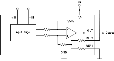
Splitting the Supply

By connecting one reference pin to V+ and the other to the ground pin, the output is set at half of the supply when there is no differential input, as shown in #SBOS4854503. This method creates a midscale offset that is ratiometric to the supply voltage; thus, if the supply increases or decreases, the output remains at half the supply.
GUID-FA05E0E1-DFED-4D32-8461-72D3922E48DD-low.gifFigure 7-5 Split-Supply Output