JAJSKH9C March   2012  – January 2021 INA282-Q1 , INA283-Q1 , INA284-Q1 , INA285-Q1 , INA286-Q1

PRODUCTION DATA  

  1. 特長
  2. アプリケーション
  3. 概要
  4. Revision History
  5. Pin Configuration and Functions
  6. Specifications
    1. 6.1 Absolute Maximum Ratings
    2. 6.2 ESD Ratings
    3. 6.3 Recommended Operating Conditions
    4. 6.4 Thermal Information
    5. 6.5 Electrical Characteristics
    6. 6.6 Typical Characteristics
  7. Detailed Description
    1. 7.1 Overview
    2. 7.2 Functional Block Diagram
    3. 7.3 Feature Description
      1. 7.3.1 Selecting RS
      2. 7.3.2 Effective Bandwidth
      3. 7.3.3 Transient Protection
    4. 7.4 Device Functional Modes
      1. 7.4.1 Reference Pin Connection Options
        1. 7.4.1.1 Unidirectional Operation
          1. 7.4.1.1.1 Ground Referenced Output
          2. 7.4.1.1.2 V+ Referenced Output
        2. 7.4.1.2 Bidirectional Operation
          1. 7.4.1.2.1 External Reference Output
          2. 7.4.1.2.2 Splitting the Supply
          3. 7.4.1.2.3 Splitting an External Reference
      2. 7.4.2 Shutdown
      3. 7.4.3 Extended Negative Common-Mode Range
      4. 7.4.4 Calculating Total Error
        1. 7.4.4.1 Example 1 INA282-Q1
        2. 7.4.4.2 Example 2 INA286-Q1
  8. Application and Implementation
    1. 8.1 Application Information
      1. 8.1.1 Basic Connections
    2. 8.2 Typical Applications
      1. 8.2.1 Current Summing
        1. 8.2.1.1 Design Requirements
        2. 8.2.1.2 Detailed Design Procedures
        3. 8.2.1.3 Application Curve
      2. 8.2.2 Current Differencing
        1. 8.2.2.1 Design Requirements
        2. 8.2.2.2 Detailed Design Procedure
        3. 8.2.2.3 Application Curve
  9. Power Supply Recommendations
  10. 10Layout
    1. 10.1 Layout Guidelines
    2. 10.2 Layout Example
  11. 11Device and Documentation Support
    1. 11.1 ドキュメントの更新通知を受け取る方法
    2. 11.2 サポート・リソース
    3. 11.3 Trademarks
    4. 11.4 静電気放電に関する注意事項
  12. 12用語集
  13. 13Mechanical, Packaging, and Orderable Information

パッケージ・オプション

メカニカル・データ(パッケージ|ピン)
サーマルパッド・メカニカル・データ
発注情報

Pin Configuration and Functions

GUID-41ADDDD7-1BC6-47BA-BFF4-30F61CE4F82B-low.gif
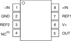
NC: This pin is not internally connected. The NC pin should either be left floating or connected to GND.
Figure 5-1 D and DGK Package8-Pin SOIC and VSSOPTop View
Table 5-1 Pin Functions
PIN I/O DESCRIPTION
NO. NAME
1 –IN Analog input Connection to negative side of shunt resistor.
2 GND Analog Ground
3 REF2 Analog input Reference voltage, 0 V to V+. See GUID-D1B20493-26A2-4F3F-8A53-6EF1AEDB7A8C.html#GUID-D1B20493-26A2-4F3F-8A53-6EF1AEDB7A8C for connection options.
4 NC This pin is not internally connected. The NC pin should either be left floating or connected to GND.
5 OUT Analog output Output voltage
6 V+ Analog Power supply, 2.7 V to 18 V
7 REF1 Analog input Reference voltage, 0 V to V+. See GUID-D1B20493-26A2-4F3F-8A53-6EF1AEDB7A8C.html#GUID-D1B20493-26A2-4F3F-8A53-6EF1AEDB7A8C for connection options.
8 +IN Analog input Connection to positive side of shunt resistor.