JAJSCZ9C September   2016  – March 2019 INA302 , INA303

PRODUCTION DATA.  

  1. 特長
  2. アプリケーション
  3. 概要
    1.     Device Images
      1.      代表的なアプリケーション
  4. 改訂履歴
  5. 概要(続き)
  6. Pin Configuration and Functions
    1.     Pin Functions
  7. Specifications
    1. 7.1 Absolute Maximum Ratings
    2. 7.2 ESD Ratings
    3. 7.3 Recommended Operating Conditions
    4. 7.4 Thermal Information
    5. 7.5 Electrical Characteristics
    6. 7.6 Typical Characteristics
  8. Detailed Description
    1. 8.1 Overview
    2. 8.2 Functional Block Diagram
    3. 8.3 Feature Description
      1. 8.3.1 Bidirectional Current Sensing
      2. 8.3.2 Out-of-Range Detection
      3. 8.3.3 Alert Outputs
        1. 8.3.3.1 Setting Alert Thresholds
          1. 8.3.3.1.1 Resistor-Controlled Current Limit
            1. 8.3.3.1.1.1 Resistor-Controlled Current Limit: Example
          2. 8.3.3.1.2 Voltage-Source-Controlled Current Limit
        2. 8.3.3.2 Hysteresis
    4. 8.4 Device Functional Modes
      1. 8.4.1 Alert Operating Modes
        1. 8.4.1.1 Transparent Output Mode
        2. 8.4.1.2 Latch Output Mode
  9. Application and Implementation
    1. 9.1 Application Information
      1. 9.1.1 Selecting a Current-Sensing Resistor (RSENSE)
        1. 9.1.1.1 Selecting a Current-Sensing Resistor: Example
      2. 9.1.2 Input Filtering
      3. 9.1.3 Using the INA30x With Common-Mode Transients Greater Than 36 V
    2. 9.2 Typical Application
      1. 9.2.1 Design Requirements
      2. 9.2.2 Detailed Design Procedure
      3. 9.2.3 Application Curve
  10. 10Power Supply Recommendations
  11. 11Layout
    1. 11.1 Layout Guidelines
    2. 11.2 Layout Example
  12. 12デバイスおよびドキュメントのサポート
    1. 12.1 ドキュメントのサポート
      1. 12.1.1 関連資料
    2. 12.2 関連リンク
    3. 12.3 ドキュメントの更新通知を受け取る方法
    4. 12.4 コミュニティ・リソース
    5. 12.5 商標
    6. 12.6 静電気放電に関する注意事項
    7. 12.7 Glossary
  13. 13メカニカル、パッケージ、および注文情報

パッケージ・オプション

メカニカル・データ(パッケージ|ピン)
サーマルパッド・メカニカル・データ
発注情報

Using the INA30x With Common-Mode Transients Greater Than 36 V

With a small amount of additional circuitry, these devices can be used in circuits subject to transients higher than 36 V. Use only zener diodes or zener-type transient absorbers (sometimes referred to as transzorbs). Any other type of transient absorber has an unacceptable time delay. Start by adding a pair of resistors as a working impedance for the zener diode, as shown in Figure 51. Keep these resistors as small as possible, preferably 10 Ω or less. Larger values can be used with an additional induced error resulting from a reduced signal that actually reaches the device input pins. Many applications are satisfied with a 10-Ω resistor along with conventional zener diodes of the lowest power rating available because this circuit limits only short-term transients. This combination uses the least amount of board space. These diodes can be found in packages as small as SOT-523 or SOD-523.
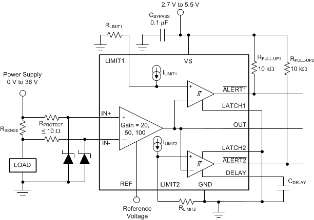
INA302 INA303 ai_transient_bos775.gifFigure 51. Transient Protection