JAJSH88A April   2019  – June 2019 INA818

PRODUCTION DATA.  

  1. 特長
  2. アプリケーション
  3. 概要
    1.     Device Images
      1.      INA818 の簡略化された内部回路図
      2.      入力段のオフセット電圧ドリフトの代表的な分布
  4. 改訂履歴
  5. Device Comparison Table
  6. Pin Configuration and Functions
    1.     Pin Functions
  7. Specifications
    1. 7.1 Absolute Maximum Ratings
    2. 7.2 ESD Ratings
    3. 7.3 Recommended Operating Conditions
    4. 7.4 Thermal Information
    5. 7.5 Electrical Characteristics
    6. 7.6 Typical Characteristics: Table of Graphs
    7. 7.7 Typical Characteristics
  8. Detailed Description
    1. 8.1 Overview
    2. 8.2 Functional Block Diagram
    3. 8.3 Feature Description
      1. 8.3.1 Setting the Gain
        1. 8.3.1.1 Gain Drift
      2. 8.3.2 EMI Rejection
      3. 8.3.3 Input Common-Mode Range
      4. 8.3.4 Input Protection
      5. 8.3.5 Operating Voltage
      6. 8.3.6 Error Sources
    4. 8.4 Device Functional Modes
  9. Application and Implementation
    1. 9.1 Application Information
      1. 9.1.1 Reference Pin
      2. 9.1.2 Input Bias Current Return Path
    2. 9.2 Typical Applications
      1. 9.2.1 Three-Pin Programmable Logic Controller (PLC)
        1. 9.2.1.1 Design Requirements
        2. 9.2.1.2 Detailed Design Procedure
        3. 9.2.1.3 Application Curves
      2. 9.2.2 Resistance Temperature Detector Interface
  10. 10Power Supply Recommendations
  11. 11Layout
    1. 11.1 Layout Guidelines
    2. 11.2 Layout Example
  12. 12デバイスおよびドキュメントのサポート
    1. 12.1 ドキュメントのサポート
      1. 12.1.1 関連資料
    2. 12.2 ドキュメントの更新通知を受け取る方法
    3. 12.3 コミュニティ・リソース
    4. 12.4 商標
    5. 12.5 静電気放電に関する注意事項
    6. 12.6 Glossary
  13. 13メカニカル、パッケージ、および注文情報

パッケージ・オプション

メカニカル・データ(パッケージ|ピン)
サーマルパッド・メカニカル・データ
発注情報

Setting the Gain

Figure 55 shows that the gain of the INA818 is set by a single external resistor (RG) connected between the RG pins (pins 1 and 8).
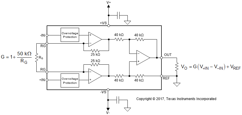
INA818 FBD_01_SBOS792.gifFigure 55. Simplified Diagram of the INA818 With Gain and Output Equations

The value of RG is selected according to Equation 1:

Equation 1. INA818 ai_eq001_SBOS792.gif

Table 2 lists several commonly-used gains and resistor values. The 50-kΩ term in Equation 1 comes from the sum of the two internal 25-kΩ feedback resistors. These on-chip resistors are laser-trimmed to accurate absolute values. The accuracy and temperature coefficients of these resistors are included in the gain accuracy and drift specifications of the INA818. As shown in Figure 55 and explained in more details in the Layout section, make sure to connect low-ESR, 0.1-µF ceramic bypass capacitors between each supply pin and ground that are placed as close to the device as possible.

Table 2. Commonly-Used Gains and Resistor Values

DESIRED GAIN RG (Ω) NEAREST 1% RG (Ω)
1 NC NC
2 50 k 49.9 k
5 12.5 k 12.4 k
10 5.556 k 5.49 k
20 2.632 k 2.61 k
50 1.02 k 1.02 k
100 505.1 511
200 251.3 249
500 100.2 100
1000 50.05 49.9