JAJSFM6A June 2018 – October 2018 ISO224
PRODUCTION DATA.
- 1 特長
- 2 アプリケーション
- 3 概要
- 4 改訂履歴
- 5 デバイス比較表
- 6 Pin Configuration and Functions
-
7 Specifications
- 7.1 Absolute Maximum Ratings
- 7.2 ESD Ratings
- 7.3 Recommended Operating Conditions
- 7.4 Thermal Information
- 7.5 Power Ratings
- 7.6 Insulation Specifications
- 7.7 Safety-Related Certifications
- 7.8 Safety Limiting Values
- 7.9 Electrical Characteristics
- 7.10 Switching Characteristics
- 7.11 Insulation Characteristics Curves
- 7.12 Typical Characteristics
- 8 Detailed Description
- 9 Application and Implementation
- 10Power Supply Recommendations
- 11Layout
- 12デバイスおよびドキュメントのサポート
- 13メカニカル、パッケージ、および注文情報
8.3.2 Input Clamp Protection Circuit
As illustrated in the Functional Block Diagram, the ISO224 features an internal clamp protection circuit on the analog input IN. Using external protection circuits is recommended as a secondary protection scheme to protect the device against surges, ESD events, and electrical fast transient (EFT) conditions.
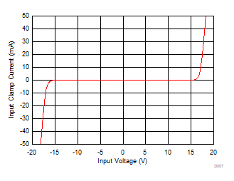
Figure 42 shows a typical current versus voltage characteristic curve for the input clamp. Limit either the voltage VIN at the input pin IN to the voltage range as defined in the Recommended Operating Conditions table or the input current to the limits as defined in the Absolute Maximum Ratings table.
 Figure 42. I-V Curve of the Input Clamp Protection Circuit
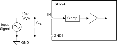
 Figure 43 shows a simple method to limit the input current with an external series resistor that is also used as part of the input low-pass filter.
 Figure 43. Series Resistor-Based Input Current Limitation on the Analog Inputs of ISO224
 The input overvoltage protection clamp on the ISO224 is intended to control transient excursions on the input pins. Leaving the device in a state such that the clamp circuit is activated for extended periods of time in normal or power-down mode is not recommended because this fault condition can degrade device performance and reliability.