SLLSFK3 november   2022 ISOW7741-Q1 , ISOW7742-Q1

PRODUCTION DATA  

  1.   1
  2. Features
  3. Applications
  4. Description
  5. Revision History
  6. Description (continued)
  7. Pin Configuration and Functions
  8. Specifications
    1. 7.1  Absolute Maximum Ratings
    2. 7.2  ESD Ratings
    3. 7.3  Recommended Operating Conditions
    4. 7.4  Thermal Information
    5. 7.5  Power Ratings
    6. 7.6  Insulation Specifications
    7. 7.7  Safety-Related Certifications
    8. 7.8  Safety Limiting Values
    9. 7.9  Electrical Characteristics - Power Converter
    10. 7.10 Supply Current Characteristics - Power Converter
    11. 7.11 Electrical Characteristics Channel Isolator - VIO, VISOIN = 5-V
    12. 7.12 Supply Current Characteristics Channel Isolator - VIO, VISOIN = 5-V
    13. 7.13 Electrical Characteristics Channel Isolator - VIO, VISOIN = 3.3-V
    14. 7.14 Supply Current Characteristics Channel Isolator - VIO, VISOIN = 3.3-V
    15. 7.15 Electrical Characteristics Channel Isolator - VIO, VISOIN = 2.5-V
    16. 7.16 Supply Current Characteristics Channel Isolator - VIO, VISOIN = 2.5-V
    17. 7.17 Electrical Characteristics Channel Isolator - VIO, VISOIN = 1.8-V
    18. 7.18 Supply Current Characteristics Channel Isolator - VIO, VISOIN = 1.8-V
    19. 7.19 Switching Characteristics - 5-V Supply
    20. 7.20 Switching Characteristics - 3.3-V Supply
    21. 7.21 Switching Characteristics - 2.5-V Supply
    22. 7.22 Switching Characteristics - 1.8-V Supply
    23. 7.23 Insulation Characteristics Curves
    24. 7.24 Typical Characteristics
  9. Parameter Measurement Information
  10. Detailed Description
    1. 9.1 Overview
      1. 9.1.1 Power Isolation
      2. 9.1.2 Signal Isolation
    2. 9.2 Functional Block Diagram
    3. 9.3 Feature Description
      1. 9.3.1 Electromagnetic Compatibility (EMC) Considerations
      2. 9.3.2 Power-Up and Power-Down Behavior
      3. 9.3.3 Protection Features
    4. 9.4 Device Functional Modes
      1. 9.4.1 Device I/O Schematics
  11. 10Application and Implementation
    1. 10.1 Application Information
    2. 10.2 Typical Application
      1. 10.2.1 Design Requirements
      2. 10.2.2 Detailed Design Procedure
      3. 10.2.3 Application Curve
      4. 10.2.4 Insulation Lifetime
  12. 11Power Supply Recommendations
  13. 12Layout
    1. 12.1 Layout Guidelines
      1. 12.1.1 PCB Material
    2. 12.2 Layout Example
  14. 13Device and Documentation Support
    1. 13.1 Device Support
    2. 13.2 Documentation Support
      1. 13.2.1 Related Documentation
    3. 13.3 Receiving Notification of Documentation Updates
    4. 13.4 Support Resources
    5. 13.5 Trademarks
    6. 13.6 Electrostatic Discharge Caution
    7. 13.7 Glossary
  15. 14Mechanical, Packaging, and Orderable Information

パッケージ・オプション

メカニカル・データ(パッケージ|ピン)
サーマルパッド・メカニカル・データ
発注情報

Typical Characteristics

GUID-20211008-SS0I-VDC2-TDBC-KN2L4Z0GTPKZ-low.svg
VSEL = GND2 TA = 25°C VISOOUT = 3.3 V
Figure 7-3 Isolated Supply Voltage (VISOOUT) vs Load Current (IISOOUT)
GUID-20211008-SS0I-VJNB-9R0M-NVJKN3HT3VBQ-low.svg
TA = 25°C
Figure 7-5 Supply Current (IDD) vs Load Current (IISOOUT)
GUID-20211011-SS0I-WPNV-WM0D-9Z4QQ9H28GS4-low.svg
TA = 25°C
Figure 7-7 Power Dissipation vs Load Current (IISOOUT)
GUID-20211008-SS0I-5GZH-XNWW-HSDLHXDVHHPW-low.svg
VSEL = VISOOUT VDD = 5 V No VISOOUT Load
Figure 7-9 5-V Isolated Supply Voltage (VISOOUT) vs Free-Air Temperature
GUID-20211008-SS0I-4SZ8-T8S3-TPDFML2QGTBC-low.svg
CL = 15 pF TA = 25°C
Figure 7-11 ISOW7741-Q1 Channel Supply Currents vs Data Rate For CL = 15 pF
GUID-20220324-SS0I-TK2C-85R1-JCGLMF49LKNS-low.svg
CL = 15 pF TA = 25°C
Figure 7-13 ISOW7742-Q1 Channel Supply Currents vs Data Rate For CL = 15 pF
GUID-20211008-SS0I-SNMJ-GJL5-7GDZ48LLBHLK-low.svgFigure 7-15 Power-Supply Undervoltage Threshold vs Free Air Temperature
GUID-20211008-SS0I-5191-1ZN2-VLZPBSXG4ZFF-low.svg
TA = 25°C
Figure 7-17 High-Level Output Voltage vs High-Level Output Current
GUID-20211008-SS0I-K4D3-0D59-TMNHJ1VSPNQ8-low.gif
VDD = 5 V VISOOUT = 3.3 V TA = 25°C
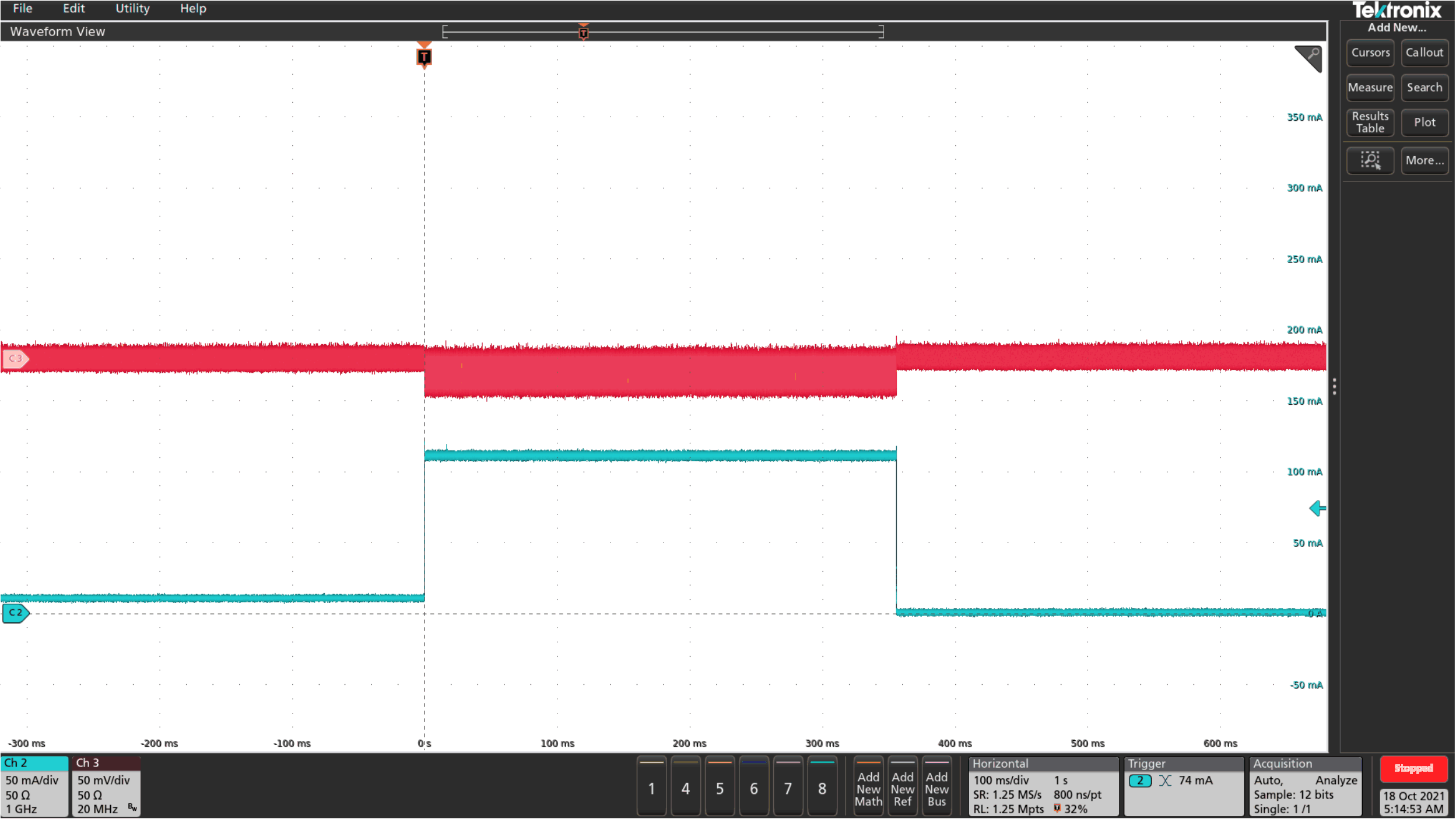
Figure 7-19 10-mA to 110-mA Load Transient Response
GUID-20211008-SS0I-WVT3-VDF4-JSXRMWGNQMRD-low.gif
VDD = 5 V VISOOUT = 3.3 V 10 uF Capacitor on VISOOUT
Figure 7-21 Soft Start at 50-mA Load For VISOOUT = 3.3 V
GUID-20211008-SS0I-2XS1-ZNMW-QFP7WFP72PZ1-low.gif
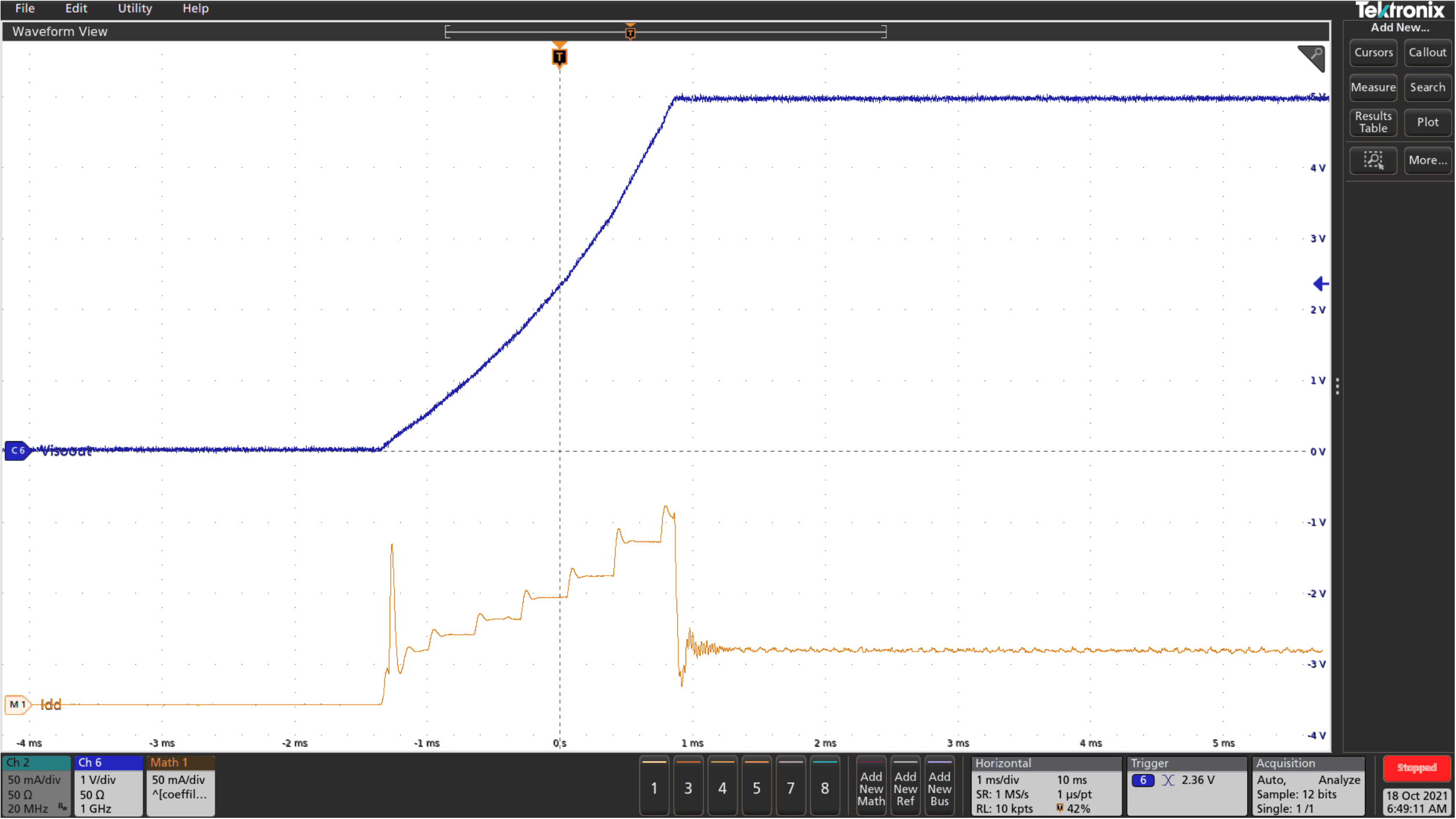
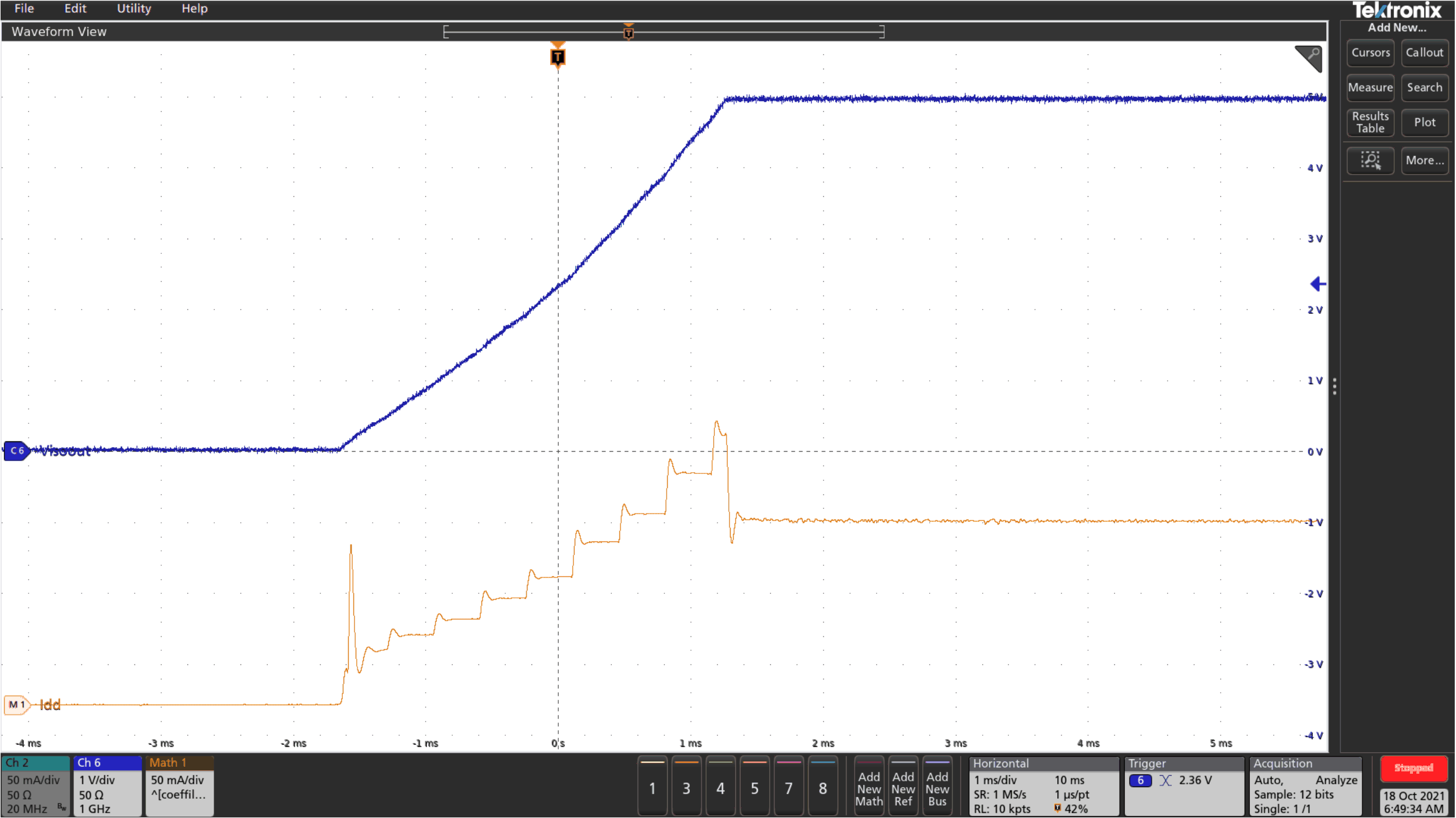
VDD = 5 V VISOOUT = 5 V 10 uF Capacitor on VISOOUT
Figure 7-23 Soft Start at 10-mA Load For VISOOUT = 5 V
GUID-20211008-SS0I-PVP3-TQLL-DVXLQPSPXQH0-low.gif
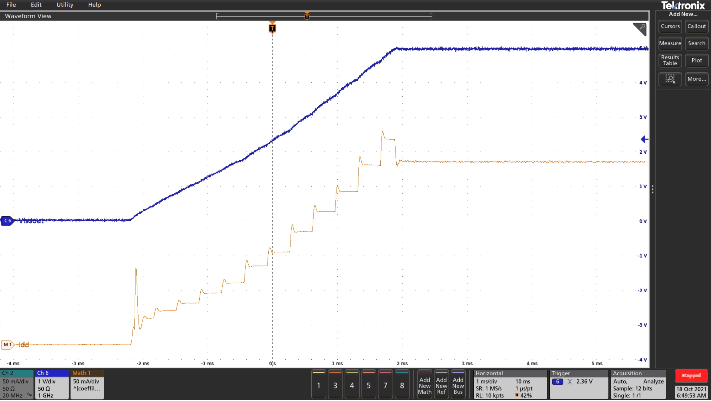
VDD = 5 V VISOOUT = 5 V 10 uF Capacitor on VISOOUT
Figure 7-25 Soft Start at 110-mA Load For VISOOUT = 5 V
GUID-20211008-SS0I-MRZM-34VJ-9JGPDHG5FTXR-low.gif
VDD = 5 V VISOOUT = 5 V 10 uF Capacitor on VISOOUT
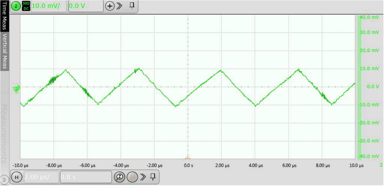
Figure 7-27 VISOOUT Ripple Voltage at 5 V with 10 uF Capacitor and 110 mA load
GUID-20211008-SS0I-DKJ6-CCRJ-BDJP1ZG0KR0G-low.gif
VDD = 5 V VISOOUT = 5 V 100 uF Capacitor on VISOOUT
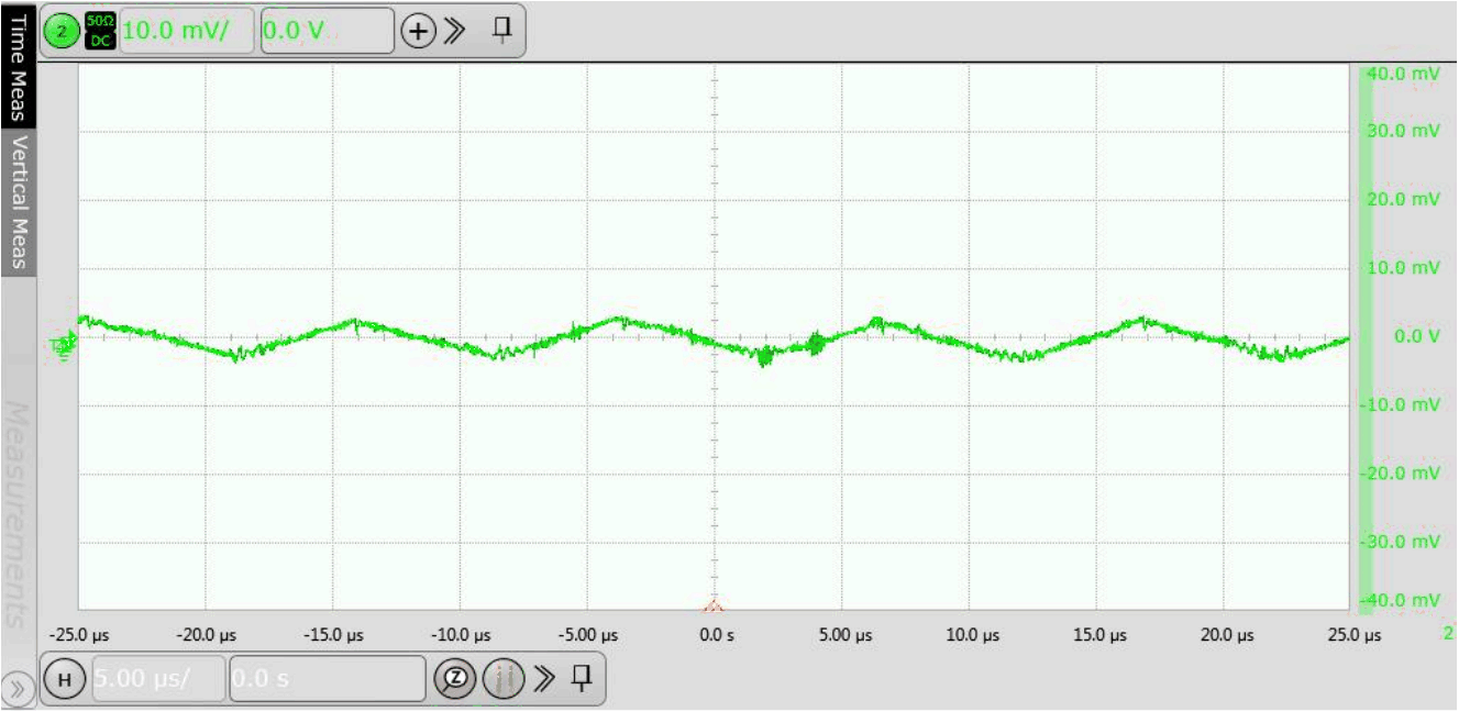
Figure 7-29 VISOOUT Ripple Voltage at 5 V with 100 uF Capacitor and 110 mA load
GUID-20211008-SS0I-3FZN-CR3R-MZV4RJJW6STF-low.svg
VSEL = VISOOUT TA = 25°C VISOOUT = 5 V
Figure 7-4 Isolated Supply Voltage (VISOOUT) vs Load Current (IISOOUT)
GUID-20211008-SS0I-F5H7-FK9B-MBGDTFPMBLQ5-low.svg
TA = 25°C
Figure 7-6 Efficiency vs Load Current (IVISOOUT)
GUID-20211008-SS0I-JHXG-ZKR6-NM59HQNZ1LM1-low.svg
VSEL = GND2 VDD = 5 V No VISOOUT Load
Figure 7-8 3.3-V Isolated Supply Voltage (VISOOUT) vs Free-Air Temperature
GUID-20211008-SS0I-QK21-QRJW-QXFG3N7VSP6F-low.svg
VSEL = VISOOUT VISOOUT = GND2 TA = 25°C = GND1
Figure 7-10 Short-Circuit Supply Current (ICC) vs Supply Voltage (VCC)
GUID-20211008-SS0I-5H8W-ZCDP-ZJCRLTRQ91BJ-low.svg
CL = 0 pF TA = 25°C
Figure 7-12 ISOW7741-Q1 Channel Supply Currents vs Data Rate For CL = 0 pF
GUID-20220324-SS0I-ZWQ0-H1MH-9RSV2VL0GD3B-low.svg
CL = 0 pF TA = 25°C
Figure 7-14 ISOW7742-Q1 Channel Supply Currents vs Data Rate For CL = 0 pF
GUID-20211015-SS0I-LJRP-MWMZ-CNLSML776J9K-low.svg
Figure 7-16 Propagation Delay Time vs Free-Air Temperature
GUID-20211008-SS0I-BD2P-7WPD-PXT5DBCHVHN2-low.svg
TA = 25°C
Figure 7-18 Low-Level Output Voltage vs Low-Level Output Current
GUID-20211008-SS0I-C3X3-FJTB-5L5ZS88B6K01-low.gif
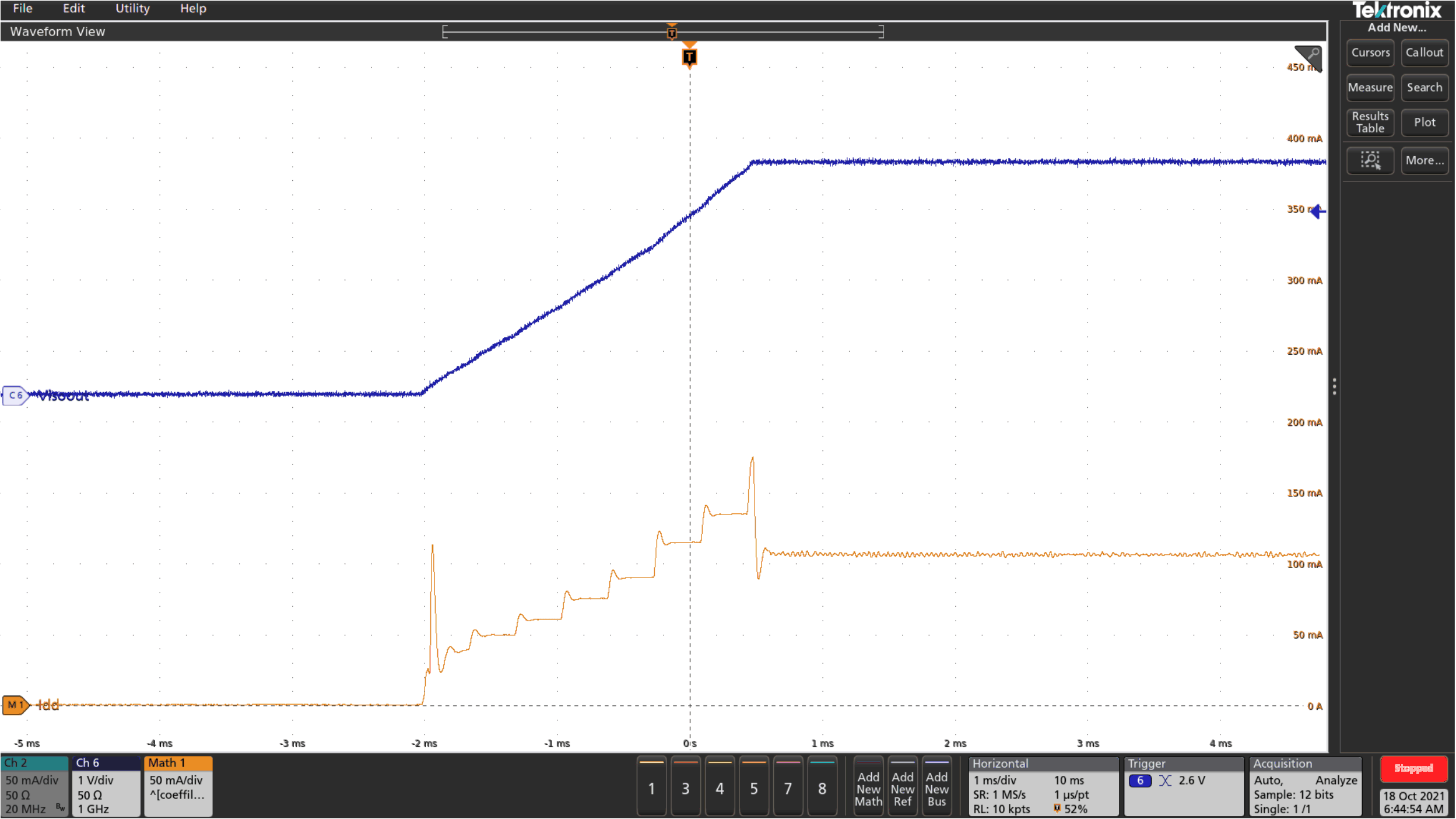
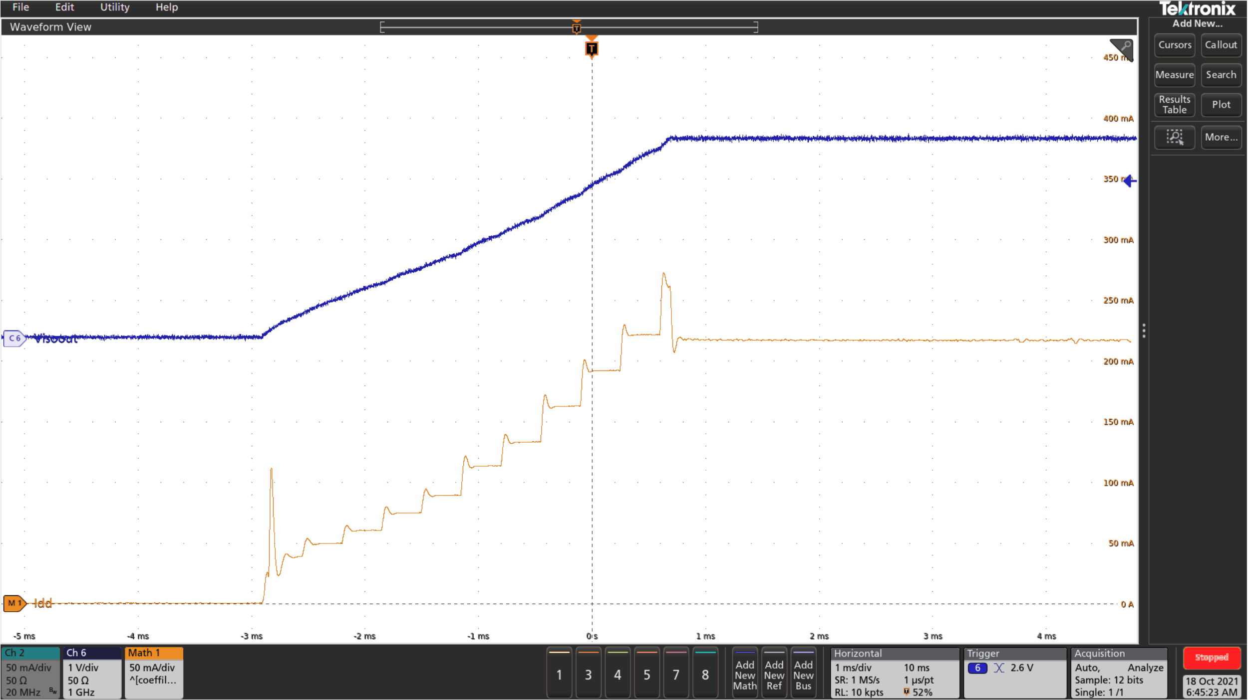
VDD = 5 V VISOOUT = 3.3 V 10 uF Capacitor on VISOOUT
Figure 7-20 Soft Start at 10-mA Load For VISOOUT = 3.3 V
GUID-20211008-SS0I-7D3Q-CTTG-K62W0SZQFLNW-low.gif
VDD = 5 V VISOOUT = 3.3 V 10 uF Capacitor on VISOOUT
Figure 7-22 Soft Start at 110-mA Load For VISOOUT = 3.3 V
GUID-20211008-SS0I-TZJ5-PXF0-WD9MQVT21QT0-low.gif
VDD = 5 V VISOOUT = 5 V 10 uF Capacitor on VISOOUT
Figure 7-24 Soft Start at 50-mA Load For VISOOUT = 5 V
GUID-20211008-SS0I-LXJP-5SKK-W4P6QNR6S8NF-low.gif
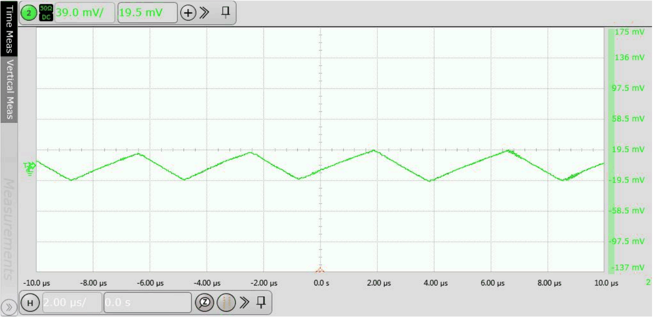
VDD = 3.3 V VISOOUT = 3.3 V 10 uF Capacitor on VISOOUT
Figure 7-26 VISOOUT Ripple Voltage at 3.3 V with 10 uF Capacitor and 60 mA load
GUID-20211008-SS0I-TB7W-4G3V-QZQTMJR9WWPS-low.gif
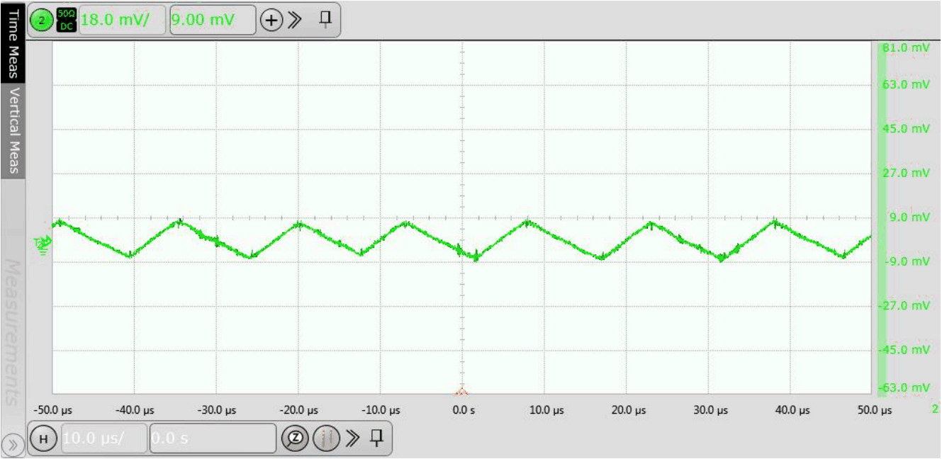
VDD = 3.3 V VISOOUT = 3.3 V 100 uF Capacitor on VISOOUT
Figure 7-28 VISOOUT Ripple Voltage at 3.3 V with 100 uF Capacitor and 60 mA load
GUID-20211020-SS0I-FHGF-MHK1-S2DMGTVSHTRN-low.svg
TA = 25°C
Figure 7-30 VISOOUT Ripple Voltage vs Load Capacitor