JAJSJ74B August   2021  – August 2023 JFE2140

PRODUCTION DATA  

  1.   1
  2. 特長
  3. アプリケーション
  4. 概要
  5. Revision History
  6. Pin Configuration and Functions
  7. Specifications
    1. 6.1 Absolute Maximum Ratings
    2. 6.2 ESD Ratings
    3. 6.3 Recommended Operating Conditions
    4. 6.4 Thermal Information
    5. 6.5 Electrical Characteristics
    6. 6.6 Typical Characteristics
  8. Parameter Measurement Information
    1. 7.1 AC Measurement Configurations
  9. Detailed Description
    1. 8.1 Overview
    2. 8.2 Functional Block Diagram
    3. 8.3 Feature Description
      1. 8.3.1 Precision Matching
      2. 8.3.2 Ultra-Low Noise
      3. 8.3.3 Low Gate Current
      4. 8.3.4 Input Protection
    4. 8.4 Device Functional Modes
  10. Application and Implementation
    1. 9.1 Application Information
      1. 9.1.1 Input Protection Diodes
      2. 9.1.2 Cascode Configuration
      3. 9.1.3 Common-Source Amplifier
      4. 9.1.4 Composite Amplifiers
    2. 9.2 Typical Applications
      1. 9.2.1 Low-Noise, Low-Power, High-Input-Impedance Composite Amplifier
        1. 9.2.1.1 Design Requirements
        2. 9.2.1.2 Detailed Design Procedure
        3. 9.2.1.3 Application Curves
      2. 9.2.2 Differential Front-End Design
        1. 9.2.2.1 Application Curves
    3. 9.3 Power Supply Recommendations
    4. 9.4 Layout
      1. 9.4.1 Layout Guidelines
      2. 9.4.2 Layout Example
  11. 10Device and Documentation Support
    1. 10.1 Device Support
      1. 10.1.1 Development Support
        1. 10.1.1.1 PSpice® for TI
        2. 10.1.1.2 TINA-TI™シミュレーション・ソフトウェア (無償ダウンロード)
        3. 10.1.1.3 TI のリファレンス・デザイン
        4. 10.1.1.4 フィルタ設計ツール
    2. 10.2 Documentation Support
      1. 10.2.1 Related Documentation
    3. 10.3 ドキュメントの更新通知を受け取る方法
    4. 10.4 サポート・リソース
    5. 10.5 Trademarks
    6. 10.6 静電気放電に関する注意事項
    7. 10.7 用語集
  12. 11Mechanical, Packaging, and Orderable Information

パッケージ・オプション

メカニカル・データ(パッケージ|ピン)
サーマルパッド・メカニカル・データ
発注情報

AC Measurement Configurations

The circuit configuration used for noise measurements is seen in Figure 7-1. The nominal IDS current is configured in the schematic by calibrating V–. After IDS is fixed, the VDS voltage is set by calibrating V+. For input-referred noise data, the gain of the circuit is calibrated from VIN to VOUT and used for the input-referred gain calculation.
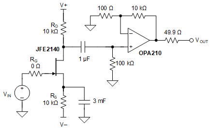
GUID-20210812-SS0I-SFV9-FR89-GPFJZH9PRVWX-low.gif Figure 7-1 AC Measurement Reference Schematic