JAJSB11H April   2009  – November 2014 LM25011 , LM25011-Q1

PRODUCTION DATA.  

  1. 特長
  2. アプリケーション
  3. 概要
    1.     代表的なアプリケーション
  4. 改訂履歴
  5. Pin Configuration and Functions
    1.     Pin Functions
  6. Specifications
    1. 6.1 Absolute Maximum Ratings
    2. 6.2 Handling Ratings: LM25011
    3. 6.3 Handling Ratings: LM25011-Q1
    4. 6.4 Recommended Operating Conditions
    5. 6.5 Thermal Information
    6. 6.6 Electrical Characteristics
    7. 6.7 Typical Characteristics
  7. Detailed Description
    1. 7.1 Overview
    2. 7.2 Functional Block Diagram
    3. 7.3 Feature Description
      1. 7.3.1 Control Circuit Overview
      2. 7.3.2 On-Time Timer
      3. 7.3.3 Current Limit
      4. 7.3.4 Ripple Requirements
      5. 7.3.5 N-Channel Buck Switch and Driver
      6. 7.3.6 Soft-Start
      7. 7.3.7 Power Good Output (PGD)
      8. 7.3.8 Thermal Shutdown
    4. 7.4 Device Functional Modes
      1. 7.4.1 Shutdown Function
  8. Application and Implementation
    1. 8.1 Application Information
    2. 8.2 Typical Application
      1. 8.2.1 LM25011 Example Circuit
        1. 8.2.1.1 Design Requirements
        2. 8.2.1.2 Detailed Design Procedure
          1. 8.2.1.2.1 Custom Design with WEBENCH Tools
          2. 8.2.1.2.2 External Components
        3. 8.2.1.3 Application Curves
      2. 8.2.2 Output Ripple Control
        1. 8.2.2.1 Option A: Lowest Cost Configuration
        2. 8.2.2.2 Option B: Intermediate VOUT Ripple Configuration
        3. 8.2.2.3 Option C: Minimum VOUT Ripple Configuration
  9. Power Supply Recommendations
  10. 10Layout
    1. 10.1 Layout Guidelines
    2. 10.2 Layout Example
    3. 10.3 Power Dissipation
  11. 11デバイスおよびドキュメントのサポート
    1. 11.1 WEBENCHツールによるカスタム設計
    2. 11.2 ドキュメントの更新通知を受け取る方法
    3. 11.3 関連リンク
    4. 11.4 商標
    5. 11.5 静電気放電に関する注意事項
    6. 11.6 Glossary
  12. 12メカニカル、パッケージ、および注文情報

パッケージ・オプション

メカニカル・データ(パッケージ|ピン)
サーマルパッド・メカニカル・データ
発注情報

Ripple Requirements

The LM25011 requires about 25 mVP-P of ripple voltage at the CS pin. Higher switching frequencies may require more ripple. That ripple voltage is generated by the decreasing recirculating current (the inductor ripple current) through RS during the off-time. See Figure 16.
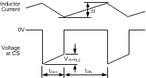
LM25011 LM25011-Q1 LM25011A LM25011A-Q1 30094625.gifFigure 16. CS Pin Waveform

The ripple voltage is equal to:

Equation 7. VRIPPLE = ΔI × RS

where ΔI is the inductor current ripple amplitude, and RS is the current-sense resistor at the CS pin.

More ripple can be achieved by decreasing the inductor value.

The LM25011A, with its shorter minimum off-time, typically will require more ripple than the LM25011. An external circuit to increase the effective ripple voltage may be needed. Different methods of generating this ripple are explained in the External Components section.