JAJSB11H April   2009  – November 2014 LM25011 , LM25011-Q1

PRODUCTION DATA.  

  1. 特長
  2. アプリケーション
  3. 概要
    1.     代表的なアプリケーション
  4. 改訂履歴
  5. Pin Configuration and Functions
    1.     Pin Functions
  6. Specifications
    1. 6.1 Absolute Maximum Ratings
    2. 6.2 Handling Ratings: LM25011
    3. 6.3 Handling Ratings: LM25011-Q1
    4. 6.4 Recommended Operating Conditions
    5. 6.5 Thermal Information
    6. 6.6 Electrical Characteristics
    7. 6.7 Typical Characteristics
  7. Detailed Description
    1. 7.1 Overview
    2. 7.2 Functional Block Diagram
    3. 7.3 Feature Description
      1. 7.3.1 Control Circuit Overview
      2. 7.3.2 On-Time Timer
      3. 7.3.3 Current Limit
      4. 7.3.4 Ripple Requirements
      5. 7.3.5 N-Channel Buck Switch and Driver
      6. 7.3.6 Soft-Start
      7. 7.3.7 Power Good Output (PGD)
      8. 7.3.8 Thermal Shutdown
    4. 7.4 Device Functional Modes
      1. 7.4.1 Shutdown Function
  8. Application and Implementation
    1. 8.1 Application Information
    2. 8.2 Typical Application
      1. 8.2.1 LM25011 Example Circuit
        1. 8.2.1.1 Design Requirements
        2. 8.2.1.2 Detailed Design Procedure
          1. 8.2.1.2.1 Custom Design with WEBENCH Tools
          2. 8.2.1.2.2 External Components
        3. 8.2.1.3 Application Curves
      2. 8.2.2 Output Ripple Control
        1. 8.2.2.1 Option A: Lowest Cost Configuration
        2. 8.2.2.2 Option B: Intermediate VOUT Ripple Configuration
        3. 8.2.2.3 Option C: Minimum VOUT Ripple Configuration
  9. Power Supply Recommendations
  10. 10Layout
    1. 10.1 Layout Guidelines
    2. 10.2 Layout Example
    3. 10.3 Power Dissipation
  11. 11デバイスおよびドキュメントのサポート
    1. 11.1 WEBENCHツールによるカスタム設計
    2. 11.2 ドキュメントの更新通知を受け取る方法
    3. 11.3 関連リンク
    4. 11.4 商標
    5. 11.5 静電気放電に関する注意事項
    6. 11.6 Glossary
  12. 12メカニカル、パッケージ、および注文情報

パッケージ・オプション

メカニカル・データ(パッケージ|ピン)
サーマルパッド・メカニカル・データ
発注情報

Option B: Intermediate VOUT Ripple Configuration

This configuration generates less ripple at VOUT than Option A by the addition of capacitor (Cff) as shown in Figure 23.

Because the output ripple is passed by Cff to the FB pin with little or no attenuation, the R1 value and VOUT ripple can be smaller than in Option A. The minimum value for R1 is calculated from:

Equation 24. LM25011 LM25011-Q1 LM25011A LM25011A-Q1 30094642.gif

where ΔI is the minimum ripple current amplitude, which occurs at minimum VIN, and VRIPPLE is the peak-to-peak ripple voltage injected at the FB pin. The minimum value for Cff is calculated from:

Equation 25. LM25011 LM25011-Q1 LM25011A LM25011A-Q1 30094643.gif

where tON(max) is the maximum on-time (at minimum VIN), and RFB1//RFB2 is the parallel equivalent of the feedback resistors.
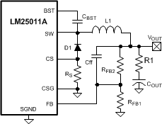
LM25011 LM25011-Q1 LM25011A LM25011A-Q1 30094641.gifFigure 23. Option B – Intermediate Ripple Configuration