JAJSEA2 December 2017 LM25574-Q1
PRODUCTION DATA.
- 1 特長
- 2 アプリケーション
- 3 概要
- 4 改訂履歴
- 5 Pin Configuration and Functions
- 6 Specifications
- 7 Detailed Description
- 8 Application and Implementation
- 9 Layout
- 10デバイスおよびドキュメントのサポート
- 11メカニカル、パッケージ、および注文情報
7.4.2 Oscillator and Sync Capability
The LM25574-Q1 oscillator frequency is set by a single external resistor connected between the RT pin and the AGND pin. The RT resistor should be located very close to the device and connected directly to the pins of the IC (RT and AGND).To set a desired oscillator frequency (F), the necessary value for the RT resistor can be calculated Equation 1:

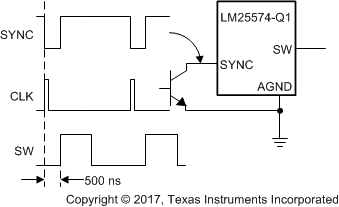
The SYNC pin can be used to synchronize the internal oscillator to an external clock. The external clock must be of higher frequency than the free-running frequency set by the RT resistor. A clock circuit with an open drain output is the recommended interface from the external clock to the SYNC pin. The clock pulse duration should be greater than 15 ns.
 Figure 9. Sync from External Clock
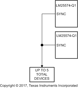
 Figure 10. Sync from Multiple Devices
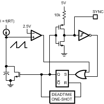
Multiple LM25574-Q1 devices can be synchronized together simply by connecting the SYNC pins together. In this configuration all of the devices will be synchronized to the highest frequency device. The diagram in Figure 11 illustrates the SYNC input/output features of the LM25574-Q1. The internal oscillator circuit drives the SYNC pin with a strong pull-down and weak pull-up inverter. When the SYNC pin is pulled low either by the internal oscillator or an external clock, the ramp cycle of the oscillator is terminated and a new oscillator cycle begins. Thus, if the SYNC pins of several LM25574-Q1 IC’s are connected together, the IC with the highest internal clock frequency will pull the connected SYNC pins low first and terminate the oscillator ramp cycles of the other IC’s. The LM25574-Q1 with the highest programmed clock frequency will serve as the master and control the switching frequency of the all the devices with lower oscillator frequency.
 Figure 11. Simplified Oscillator Block Diagram and SYNC I/O Circuit