JAJSAY9L February   2009  – May 2018 LM26420

PRODUCTION DATA.  

  1. 特長
  2. アプリケーション
  3. 概要
    1.     Device Images
      1.      LM26420デュアル降圧DC/DCコンバータ
      2.      LM26420の効率(最高93%)
  4. 改訂履歴
  5. Pin Configuration and Functions
    1.     Pin Functions: 16-Pin WQFN
    2.     Pin Functions 20-Pin HTSSOP
  6. Specifications
    1. 6.1 Absolute Maximum Ratings
    2. 6.2 ESD Ratings (LM26420X/Y)
    3. 6.3 Recommended Operating Conditions
    4. 6.4 Thermal Information
    5. 6.5 Electrical Characteristics Per Buck
    6. 6.6 Typical Characteristics
  7. Detailed Description
    1. 7.1 Overview
    2. 7.2 Functional Block Diagram
    3. 7.3 Feature Description
      1. 7.3.1 Soft Start
      2. 7.3.2 Power Good
      3. 7.3.3 Precision Enable
    4. 7.4 Device Functional Modes
      1. 7.4.1 Output Overvoltage Protection
      2. 7.4.2 Undervoltage Lockout
      3. 7.4.3 Current Limit
      4. 7.4.4 Thermal Shutdown
  8. Application and Implementation
    1. 8.1 Application Information
      1. 8.1.1 Programming Output Voltage
      2. 8.1.2 VINC Filtering Components
      3. 8.1.3 Using Precision Enable and Power Good
      4. 8.1.4 Overcurrent Protection
    2. 8.2 Typical Applications
      1. 8.2.1 LM26420X 2.2-MHz, 0.8-V Typical High-Efficiency Application Circuit
        1. 8.2.1.1 Design Requirements
        2. 8.2.1.2 Detailed Design Procedure
          1. 8.2.1.2.1 Custom Design With WEBENCH® Tools
          2. 8.2.1.2.2 Inductor Selection
          3. 8.2.1.2.3 Input Capacitor Selection
          4. 8.2.1.2.4 Output Capacitor
          5. 8.2.1.2.5 Calculating Efficiency and Junction Temperature
        3. 8.2.1.3 Application Curves
      2. 8.2.2 LM26420X 2.2-MHz, 1.8-V Typical High-Efficiency Application Circuit
        1. 8.2.2.1 Design Requirements
        2. 8.2.2.2 Detailed Design Procedure
        3. 8.2.2.3 Application Curves
      3. 8.2.3 LM26420X 2.2-MHz, 2.5-V Typical High-Efficiency Application Circuit
        1. 8.2.3.1 Design Requirements
        2. 8.2.3.2 Detailed Design Procedure
        3. 8.2.3.3 Application Curves
      4. 8.2.4 LM26420Y 550 kHz, 0.8-V Typical High-Efficiency Application Circuit
        1. 8.2.4.1 Design Requirements
        2. 8.2.4.2 Detailed Design Procedure
        3. 8.2.4.3 Application Curves
      5. 8.2.5 LM26420Y 550-kHz, 1.8-V Typical High-Efficiency Application Circuit
        1. 8.2.5.1 Design Requirements
        2. 8.2.5.2 Detailed Design Procedure
        3. 8.2.5.3 Application Curves
      6. 8.2.6 LM26420Y 550-kHz, 2.5-V Typical High-Efficiency Application Circuit
        1. 8.2.6.1 Design Requirements
        2. 8.2.6.2 Detailed Design Procedure
        3. 8.2.6.3 Application Curves
  9. Power Supply Recommendations
  10. 10Layout
    1. 10.1 Layout Guidelines
    2. 10.2 Layout Example
    3. 10.3 Thermal Considerations
      1. 10.3.1 Method 1: Silicon Junction Temperature Determination
      2. 10.3.2 Thermal Shutdown Temperature Determination
  11. 11デバイスおよびドキュメントのサポート
    1. 11.1 デバイス・サポート
      1. 11.1.1 デベロッパー・ネットワークの製品に関する免責事項
      2. 11.1.2 WEBENCH®ツールによるカスタム設計
    2. 11.2 ドキュメントのサポート
      1. 11.2.1 関連資料
    3. 11.3 ドキュメントの更新通知を受け取る方法
    4. 11.4 コミュニティ・リソース
    5. 11.5 商標
    6. 11.6 静電気放電に関する注意事項
    7. 11.7 Glossary
  12. 12メカニカル、パッケージ、および注文情報

パッケージ・オプション

メカニカル・データ(パッケージ|ピン)
サーマルパッド・メカニカル・データ
発注情報

Soft Start

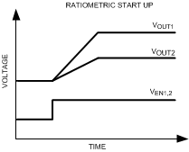
This function forces VOUT to increase at a controlled rate during start-up in a controlled fashion, which helps reduce inrush current and eliminate overshoot on VOUT. During soft start, reference voltage of the error amplifier ramps from 0 V to its nominal value of 0.8 V in approximately 600 µs. If the converter is turned on into a pre-biased load, then the feedback begins ramping from the prebias voltage but at the same rate as if it had started from 0 V. The two outputs start up ratiometrically if enabled at the same time, see Figure 28 below.
LM26420 LM26420_Soft_Start.gif
Figure 28. LM26420 Soft-Start