JAJS639K April 2000 – June 2016 LM2670
PRODUCTION DATA.
- 1 特長
- 2 アプリケーション
- 3 概要
- 4 改訂履歴
- 5 Pin Configuration and Functions
-
6 Specifications
- 6.1 Absolute Maximum Ratings
- 6.2 ESD Ratings
- 6.3 Recommended Operating Conditions
- 6.4 Thermal Information
- 6.5 Electrical Characteristics - 3.3 V
- 6.6 Electrical Characteristics - 5 V
- 6.7 Electrical Characteristics - 12 V
- 6.8 Electrical Characteristics - All Output Voltage Versions
- 6.9 Typical Characteristics
- 7 Detailed Description
- 8 Application and Implementation
- 9 Power Supply Recommendations
- 10Layout
- 11デバイスおよびドキュメントのサポート
- 12メカニカル、パッケージ、および注文情報
パッケージ・オプション
メカニカル・データ(パッケージ|ピン)
サーマルパッド・メカニカル・データ
- KTW|7
発注情報
7 Detailed Description
7.1 Overview
The LM2670 provides all of the active functions required for a step-down (buck) switching regulator. The internal power switch is a DMOS power MOSFET to provide power supply designs with high current capability, up to 3 A, and highly efficient operation.
The design support WEBENCH, can also be used to provide instant component selection, circuit performance calculations for evaluation, a bill of materials component list and a circuit schematic for LM2670.
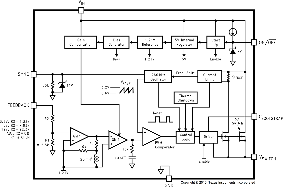
7.2 Functional Block Diagram

† Active Capacitor Patent Number 5,382,918
7.3 Feature Description
7.3.1 Switch Output
This is the output of a power MOSFET switch connected directly to the input voltage. The switch provides energy to an inductor, an output capacitor, and the load circuitry under control of an internal pulse-width-modulator (PWM). The PWM controller is internally clocked by a fixed 260-kHz oscillator. In a standard step-down application the duty cycle (Time ON/Time OFF) of the power switch is proportional to the ratio of the power supply output voltage to the input voltage. The voltage on pin 1 switches between VIN (switch ON) and below ground by the voltage drop of the external Schottky diode (switch OFF).
7.3.2 Input
The input voltage for the power supply is connected to pin 2. In addition to providing energy to the load the input voltage also provides bias for the internal circuitry of the LM2670. For ensured performance the input voltage must be in the range of 8 V to 40 V. For best performance of the power supply the input pin must always be bypassed with an input capacitor located close to pin 2.
7.3.3 C Boost
A capacitor must be connected from pin 3 to the switch output, pin 1. This capacitor boosts the gate drive to the internal MOSFET above VIN to fully turn it ON. This minimizes conduction losses in the power switch to maintain high efficiency. The recommended value for C Boost is 0.01 µF.
7.3.4 Ground
This is the ground reference connection for all components in the power supply. In fast-switching, high-current applications such as those implemented with the LM2670, TI recommends using a broad ground plane to minimize signal coupling throughout the circuit.
7.3.5 SYNC
This input allows control of the switching clock frequency. If left open-circuited the regulator will be switched at the internal oscillator frequency, between 225 kHz and 280 kHz. An external clock can be used to force the switching frequency and thereby control the output ripple frequency of the regulator. This capability provides for consistent filtering of the output ripple from system to system as well as precise frequency spectrum positioning of the ripple frequency which is often desired in communications and radio applications. This external frequency must be greater than the LM2670 internal oscillator frequency, which could be as high as 280 kHz, to prevent an erroneous reset of the internal ramp oscillator and PWM control of the power switch. The ramp oscillator is reset on the positive going edge of the sync input signal. TI recommends that the external TTL or CMOS compatible clock (between 0 V and a level greater than 3 V) be AC-coupled to the sync input through a 100-pf capacitor and a 1-kΩ resistor to ground at pin 5 as shown in Figure 21.
When the SYNC function is used, current limit frequency foldback is not active. Therefore, the device my not be fully protected against extreme output short-circuit conditions. See Additional Application Information.
7.3.6 Feedback
This is the input to a two-stage high gain amplifier, which drives the PWM controller. It is necessary to connect pin 6 to the actual output of the power supply to set the DC output voltage. For the fixed output devices (3.3-V, 5-V, and 12-V outputs), a direct wire connection to the output is all that is required as internal gain setting resistors are provided inside the LM2670. For the adjustable output version two external resistors are required to set the DC output voltage. For stable operation of the power supply it is important to prevent coupling of any inductor flux to the feedback input.
7.3.7 ON/OFF
This input provides an electrical ON/OFF control of the power supply. Connecting this pin to ground or to any voltage less than 0.8 V will completely turn OFF the regulator. The current drain from the input supply when OFF is only 50 µA. Pin 7 has an internal pull-up current source of approximately 20 µA and a protection clamp Zener diode of 7 V to ground. When electrically driving the ON/OFF pin the high voltage level for the ON condition should not exceed the 6-V absolute maximum limit. When ON/OFF control is not required pin 7 should be left open circuited.
7.4 Device Functional Modes
7.4.1 Shutdown Mode
The ON/OFF pin provides electrical ON and OFF control for the LM2670. When the voltage of this pin is lower than 1.4 V, the device is shutdown mode. The typical standby current in this mode is 50 µA.
7.4.2 Active Mode
When the voltage of the ON/OFF pin is higher than 1.4 V, the device starts switching and the output voltage rises until it reaches a normal regulation voltage.