SNAS555D June 2000 – December 2016 LM2907-N , LM2917-N
PRODUCTION DATA.
- 1 Features
- 2 Applications
- 3 Description
- 4 Revision History
- 5 Description (continued)
- 6 Pin Configuration and Functions
- 7 Specifications
- 8 Parameter Measurement Information
- 9 Detailed Description
-
10Application and Implementation
- 10.1 Application Information
- 10.2
Typical Applications
- 10.2.1 Minimum Component Tachometer
- 10.2.2
Other Application Circuits
- 10.2.2.1 Variable Reluctance Magnetic Pickup Buffer Circuits
- 10.2.2.2 Finger Touch or Contact Switch
- 10.2.2.3 Over-Speed Latch
- 10.2.2.4 Frequency Switch Applications
- 10.2.2.5 Anti-Skid Circuits
- 10.2.2.6 Changing the Output Voltage for an Input Frequency of Zero
- 10.2.2.7 Changing Tachometer Gain Curve or Clamping the Minimum Output Voltage
- 11Power Supply Recommendations
- 12Layout
- 13Device and Documentation Support
- 14Mechanical, Packaging, and Orderable Information
パッケージ・オプション
メカニカル・データ(パッケージ|ピン)
サーマルパッド・メカニカル・データ
発注情報
9 Detailed Description
9.1 Overview
The LM29x7 frequency-to-voltage converter features two separate inputs to monitor the signal. In the 8-pin devices, one of these inputs is internally grounded and therefore it monitors the remaining input for zero crossings. In the 14-pin devices, both of these inputs are open and it instead detects whenever the differential voltage switches polarity. Therefore, the input comparator outputs a square wave of equal frequency to the input.
A charge pump system is used to translate the frequency of this square wave to a voltage. At the start of every positive half cycle of the input signal a 180-µA constant current charges C1 until its voltage has increased by VCC/2. The capacitor is held at that voltage until the input signal begins a negative half cycle. Then the 180-µA constant current discharges capacitor C1 until its voltage has dropped by VCC/2. This voltage is held until the next positive half cycle and the process repeats. This generates pulses of current flowing into and out of capacitor C1 at the same frequency as the input signal. For every full cycle, the charge pump mirrors both current pulses as positive current pulses into the parallel combination of resistor R1 and capacitor C2. Therefore every full cycle, the amount of charge leaving pin 3 is equal to the sum of the charge entering C1 and leaving C1. Because the voltage at pin 3 is equal to I3(avg) × R1, I(avg) is calculated in Equation 1.
This average current will be flowing across R1, giving the output voltage in Equation 2.
C2 acts as a filter to smooth the pulses of current and does not affect the output voltage. However, the size of C2 determines both the output response time for changes in frequency and the amount of output voltage ripple.
The voltage generated is then fed in a high gain op amp. This op amp drives a bipolar transistor whose collector and emitter are each broken out to a pin. The LM29x7 has the flexibility to be configured a variety of ways to meet system requirements including voltage output, driving loads, operating a relay, and more.
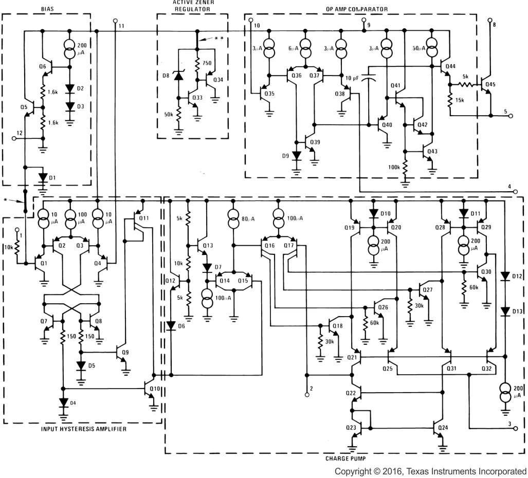
9.2 Functional Block Diagram

9.3 Feature Description
9.3.1 Differential Input
This device features a Schmitt-Trigger comparator that is the first stage in converting the input signal. Every time the output of the comparator flips between high and low correlates to a half cycle elapsing on the input signal. On the LM29x7-8 devices, one terminal of this comparator is internally connected to ground. This requires that the input signal cross zero volts in order for device to detect the frequency. On the LM29x7 devices, the input terminals to the Schmitt-Trigger comparator are both available for use. This open terminal allows the potential at which the comparator’s output is flipped to be applied externally. This allows the device to accept signals with DC offset or compare differential inputs.
9.3.2 Configurable
While the ratio of output voltage to input frequency is dependent on supply voltage, it is easily adjusted through the combination of one resistor and one capacitor, R1 and C1. The formula for calculating the expected output voltage is in Equation 3.
The sizes of R1 and C1 have other effects on the system such as maximum frequency and output linearity. See Choosing R1 and C1 for detailed instructions on sizing components.
9.3.3 Output Stage
The output voltage generated by the charge pump is fed in the noninverting terminal of a high gain op amp. This op amp then drives and uncommitted bipolar junction transistor. This allows the LM2907 to be configured a variety of ways to meet system needs. The output voltage can be buffered and used to drive a load (see Figure 15) or an output threshold can be given to trigger a load switch (see Figure 18).
9.4 Device Functional Modes
9.4.1 Grounded Input Devices (8-Pin LM2907 and LM2917)
These devices have one of the two Schmitt-Trigger comparator inputs internally grounded and must be externally connected to the system ground as well. This configuration monitors the remaining terminal for zero crossings.
9.4.2 Differential Input Devices (LM2907 and LM2917)
These devices have both inputs to the Schmitt-Trigger comparator available and broken out to pins 1 and 11. This configuration allows a new switching threshold provided in the case of signals with DC offset or to intake a differential pair and switch based on voltage difference.