SLCS007K September 1973 – March 2017 LM111 , LM211 , LM311
PRODUCTION DATA.
- 1 Features
- 2 Applications
- 3 Description
- 4 Revision History
- 5 Pin Configuration and Functions
- 6 Specifications
- 7 Parameter Measurement Information
- 8 Detailed Description
- 9 Application and Implementation
- 10Power Supply Recommendations
- 11Layout
- 12Device and Documentation Support
- 13Mechanical, Packaging, and Orderable Information
パッケージ・オプション
デバイスごとのパッケージ図は、PDF版データシートをご参照ください。
メカニカル・データ(パッケージ|ピン)
- D|8
- P|8
- PS|8
- PW|8
サーマルパッド・メカニカル・データ
- PS|8
発注情報
9 Application and Implementation
NOTE
Information in the following applications sections is not part of the TI component specification, and TI does not warrant its accuracy or completeness. TI’s customers are responsible for determining suitability of components for their purposes. Validate and test the design implementation to confirm system functionality.
9.1 Application Information
A typical LMx11 application compares a single signal to a reference or two signals against each other. Many users take advantage of the open-drain output to drive the comparison logic output to a logic voltage level to an MCU or logic device. The wide supply range and high voltage capability makes LMx11 optimal for level shifting to a higher or lower voltage.
9.2 Typical Application
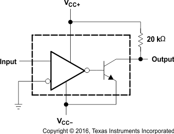 Figure 13. Zero-Crossing Detector
9.2.1 Design Requirements
For this design example, use the parameters listed in Table 1 as the input parameters.
Table 1. Design Parameters
| PARAMETER | MIN | TYP | MAX | UNIT | |
|---|---|---|---|---|---|
| VIN | Input voltage range | –15 | 13 | V | |
| VCC+ | Positive supply voltage | 15 | V | ||
| VCC– | Negative supply voltage | –15 | |||
| IOUT | Output current | 20 | mA | ||
9.2.2 Detailed Design Procedure
When using LMx11 in a general comparator application, determine the following:
- Input voltage range
- Minimum overdrive voltage
- Output and drive current
- Response time
9.2.2.1 Input Voltage Range
When choosing the input voltage range, consider the input common mode voltage range (VICR). Operation outside of this range can yield incorrect comparisons.
The following list describes the outcomes of some input voltage situations.
- When both IN– and IN+ are both within the common-mode range:
- If IN– is higher than IN+ and the offset voltage, the output is low and the output transistor is sinking current
- If IN– is lower than IN+ and the offset voltage, the output is high impedance and the output transistor is not conducting
- When IN– is higher than common mode and IN+ is within common mode, the output is low and the output transistor is sinking current
- When IN+ is higher than common mode and IN– is within common mode, the output is high impedance and the output transistor is not conducting
- When IN– and IN+ are both higher than common mode, the output is undefined
9.2.2.2 Minimum Overdrive Voltage
Overdrive voltage is the differential voltage produced between the positive and negative inputs of the comparator over the offset voltage (VIO). To make an accurate comparison the Overdrive voltage (VOD) must be higher than the input offset voltage (VIO). Overdrive voltage can also determine the response time of the comparator, with the response time decreasing with increasing overdrive. Figure 14 and Figure 15 show positive and negative response times with respect to overdrive voltage.
9.2.2.3 Output and Drive Current
Output current is determined by the pullup resistance and pullup voltage. The output current produces a output low voltage (VOL) from the comparator, in which VOL is proportional to the output current. Use Figure 5 to determine VOL based on the output current.
The output current can also effect the transient response.
9.2.2.4 Response Time
The load capacitance (CL), pullup resistance (RPULLUP), and equivalent collector-emitter resistance (RCE) levels determine the transient response. Equation 1 approximates the positive response time. Equation 2 approximates the negative response time. RCE can be determine by taking the slope of Figure 5 in the linear region at the desired temperature, or by Equation 3.


where
- VOL is the low-level output voltage
- IOUT is the output current
9.2.3 Application Curves
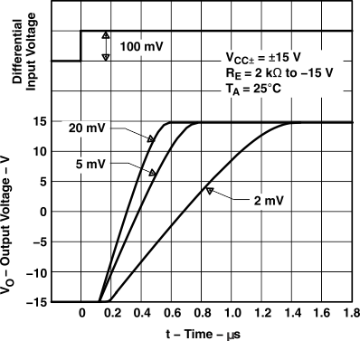 Figure 14. Output Response for Various Input Overdrives
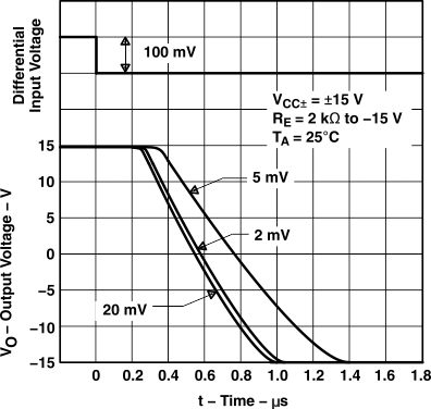 Figure 15. Output Response for Various Input Overdrives
9.3 System Examples
Figure 16 through Figure 33 show various applications for the LM111, LM211, and LM311 comparators.
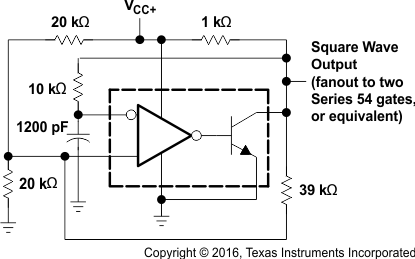 Figure 16. 100-kHz Free-Running Multivibrator
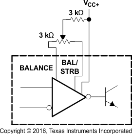
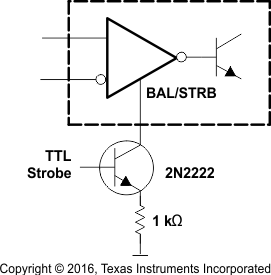
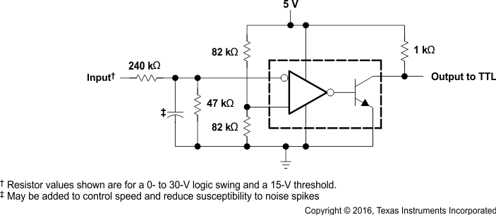 Figure 19. TTL Interface With High-Level Logic
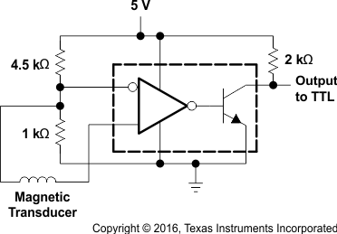 Figure 20. Detector for Magnetic Transducer
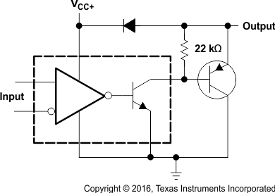 Figure 22. Comparator and Solenoid Driver
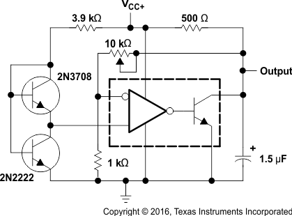 Figure 24. Low-Voltage Adjustable Reference Supply
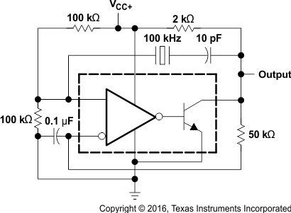 Figure 21. 100-kHz Crystal Oscillator
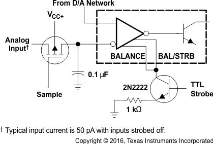 Figure 23. Strobing Both Input and Output Stages Simultaneously
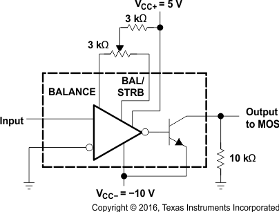 Figure 25. Zero-Crossing Detector Driving MOS Logic
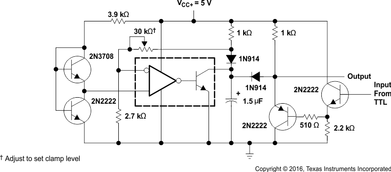 Figure 26. Precision Squarer
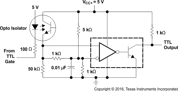 Figure 27. Digital Transmission Isolator
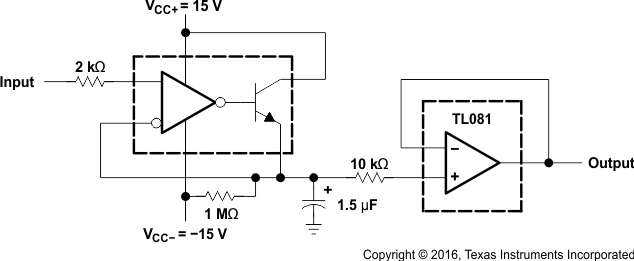 Figure 28. Positive-Peak Detector
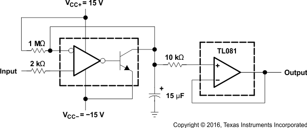 Figure 29. Negative-Peak Detector
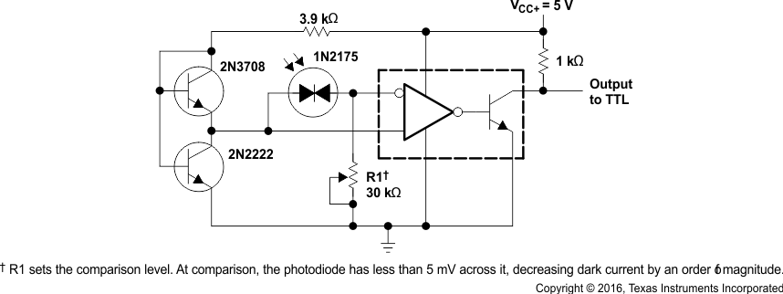 Figure 30. Precision Photodiode Comparator
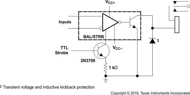 Figure 31. Relay Driver With Strobe
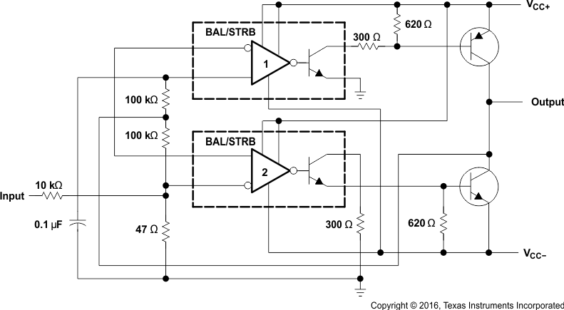 Figure 32. Switching Power Amplifier
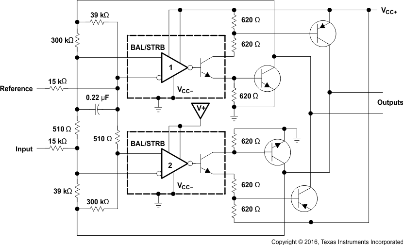 Figure 33. Switching Power Amplifiers