SLCS007K September 1973 – March 2017 LM111 , LM211 , LM311
PRODUCTION DATA.
- 1 Features
- 2 Applications
- 3 Description
- 4 Revision History
- 5 Pin Configuration and Functions
- 6 Specifications
- 7 Parameter Measurement Information
- 8 Detailed Description
- 9 Application and Implementation
- 10Power Supply Recommendations
- 11Layout
- 12Device and Documentation Support
- 13Mechanical, Packaging, and Orderable Information
パッケージ・オプション
デバイスごとのパッケージ図は、PDF版データシートをご参照ください。
メカニカル・データ(パッケージ|ピン)
- D|8
- P|8
- PS|8
- PW|8
サーマルパッド・メカニカル・データ
- PS|8
発注情報
8 Detailed Description
8.1 Overview
The LM111, LM211 and LM311 are voltage comparators that have input currents nearly a thousand times lower than legacy standard devices. They are also designed to operate over a wider range of supply voltages: from standard ±15V op amp supplies down to the single 5-V supply used for IC logic. Their output is compatible with RTL, DTL and TTL as well as MOS circuits. Further, they can drive lamps or relays, switching voltages up to 50 V at currents as high as 50 mA.
Both the inputs and the outputs of the LM111, LM211 or the LM311 can be isolated from system ground, and the output can drive loads referred to ground, the positive supply or the negative supply. Offset balancing and strobe capability are provided and outputs can be wire ORed. The LM211 is identical to the LM111, except that its performance is specified over a −40°C to +85°C temperature range instead of −55°C to +125°C. The LM311 has a temperature range of 0°C to +70°C. The LM211Q has a temperature range of −40°C to +125°C.
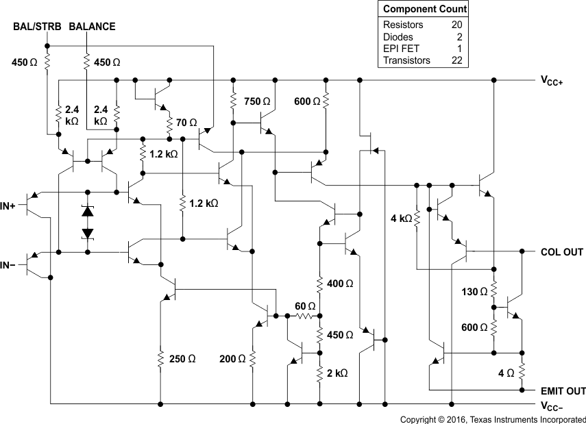
8.2 Functional Block Diagram

8.3 Feature Description
LMx11 consists of a PNP input stage to sense voltages near VCC–. It also contains balance and strobe pins for external offset adjustment or trimming.
The input stage is followed by a very high gain stage for very fast response after a voltage difference on the input pins have been sensed.
This is then followed by the output stage that consists of an open collector NPN (pulldown or low-side) transistor. Unlike most open drain comparators, this NPN output stage has an isolated emitter from VCC–, allowing this device to set the VOL output value for collector output.
8.4 Device Functional Modes
8.4.1 Voltage Comparison
The LMx11 operates solely as a voltage comparator, comparing the differential voltage between the positive and negative pins and outputting a logic low or high impedance (logic high with pullup) based on the input differential polarity.