SNVSAC2A March 2015 – June 2020 LM317A
PRODUCTION DATA.
- 1 Features
- 2 Applications
- 3 Description
- 4 Device Comparison Table
- 5 Pin Configuration and Functions
- 6 Specifications
- 7 Detailed Description
-
8 Application and Implementation
- 8.1 Application Information
- 8.2
Typical Applications
- 8.2.1 1.25-V to 25-V Adjustable Regulator
- 8.2.2 5-V Logic Regulator With Electronic Shutdown
- 8.2.3 Slow Turnon 15-V Regulator
- 8.2.4 Adjustable Regulator With Improved Ripple Rejection
- 8.2.5 High-Stability 10-V Regulator
- 8.2.6 High-Current Adjustable Regulator
- 8.2.7 Emitter-Follower Current Amplifier
- 8.2.8 1-A Current Regulator
- 8.2.9 Common-Emitter Amplifier
- 8.2.10 Low-Cost 3-A Switching Regulator
- 8.2.11 Current-Limited Voltage Regulator
- 8.2.12 Adjusting Multiple On-Card Regulators With Single Control
- 8.2.13 AC Voltage Regulator
- 8.2.14 12-V Battery Charger
- 8.2.15 Adjustable 4-A Regulator
- 8.2.16 Current-Limited 6-V Charger
- 8.2.17 Digitally-Selected Outputs
- 9 Power Supply Recommendations
- 10Layout
- 11Device and Documentation Support
- 12Mechanical, Packaging, and Orderable Information
パッケージ・オプション
メカニカル・データ(パッケージ|ピン)
サーマルパッド・メカニカル・データ
発注情報
10.1.1.2.1 Heatsinking the SOT-223 (DCY) Package
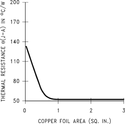
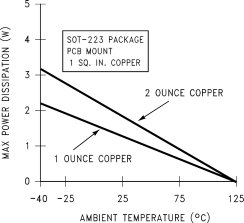
Figure 37 and Figure 38 show the information for the SOT-223 package. Figure 38 assumes a θJA of 74°C/W for 1-oz. copper and 59.6°C/W for 2-oz. copper and a maximum junction temperature of 125°C. See the AN-1028 Maximum Power Enhancement Techniques for Power Packages application note for thermal enhancement techniques to be used with SOT-223 and TO-252 packages.
 Figure 37. θJA vs Copper (2-oz.) Area for the SOT-223 Package
  Figure 38. Maximum Power Dissipation vs TAMB for the SOT-223 Package