JAJSFC4 April 2018 LM3478Q-Q1
PRODUCTION DATA.
- 1 特長
- 2 アプリケーション
- 3 概要
- 4 改訂履歴
- 5 Pin Configuration and Functions
- 6 Specifications
- 7 Detailed Description
-
8 Application and Implementation
- 8.1 Application Information
- 8.2
Typical Applications
- 8.2.1
Typical High Efficiency Step-Up (Boost) Converter
- 8.2.1.1 Design Requirements
- 8.2.1.2
Detailed Design Procedure
- 8.2.1.2.1 Custom Design with WEBENCH Tools
- 8.2.1.2.2 Power Inductor Selection
- 8.2.1.2.3 Programming the Output Voltage
- 8.2.1.2.4 Setting the Current Limit
- 8.2.1.2.5 Current Limit with External Slope Compensation
- 8.2.1.2.6 Power Diode Selection
- 8.2.1.2.7 Power MOSFET Selection
- 8.2.1.2.8 Input Capacitor Selection
- 8.2.1.2.9 Output Capacitor Selection
- 8.2.1.2.10 Compensation
- 8.2.1.3 Application Curves
- 8.2.2 Typical SEPIC Converter
- 8.2.1
Typical High Efficiency Step-Up (Boost) Converter
- 9 Power Supply Recommendations
- 10Layout
- 11デバイスおよびドキュメントのサポート
- 12メカニカル、パッケージ、および注文情報
7.3.1 Overvoltage Protection
The LM3478Q-Q1 has over voltage protection (OVP) for the output voltage. OVP is sensed at the feedback pin (pin 3). If at anytime the voltage at the feedback pin rises to VFB+ VOVP, OVP is triggered. See Electrical Characteristics section for limits on VFB and VOVP.
OVP will cause the drive pin to go low, forcing the power MOSFET off. With the MOSFET off, the output voltage will drop. TheLM3478Q-Q1 begins switching again when the feedback voltage reaches VFB + (VOVP - VOVP(HYS)). See Electrical Characteristics for limits on VOVP(HYS).
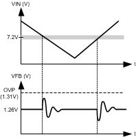
OVP can be triggered if the unregulated input voltage crosses 7.2 V, the output voltage will react as shown in Figure 21. The internal bias of the LM3478Q-Q1 comes from either the internal LDO as shown in the block diagram or the voltage at the Vin pin is used directly. At Vin voltages lower than 7.2 V the internal IC bias is the Vin voltage and at voltages above 7.2V the internal LDO of the LM3478Q-Q1 provides the bias. At the switch over threshold at 7.2 V a sudden small change in bias voltage is seen by all the internal blocks of the LM3478Q-Q1. The control voltage shifts because of the bias change, the PWM comparator tries to keep regulation. To the PWM comparator, the scenario is identical to a step change in the load current, so the response at the output voltage is the same as would be observed in a step load change. Hence, the output voltage overshoot here can also trigger OVP. The LM3478Q-Q1 will regulate in hysteretic mode for several cycles, or may not recover and simply stay in hysteretic mode until the load current drops or Vin is not crossing the 7.2 V threshold anymore. Note that the output is still regulated in hysteretic mode.
Depending on the requirements of the application, there is some influence one has over this effect. The threshold of 7.2 V can be shifted to higher voltages by adding a resistor in series with VIN. In case VIN is right at the threshold of 7.2 V, the threshold could cross over and over due to some slight ripple on VIN. To minimize the effect on the output voltage one can filter the VIN pin with an RC filter.
 Figure 21. The Feedback Voltage Experiences an Oscillation if the Input Voltage crosses the 7.2-V Internal Bias Threshold