JAJSFC4 April 2018 LM3478Q-Q1
PRODUCTION DATA.
- 1 特長
- 2 アプリケーション
- 3 概要
- 4 改訂履歴
- 5 Pin Configuration and Functions
- 6 Specifications
- 7 Detailed Description
-
8 Application and Implementation
- 8.1 Application Information
- 8.2
Typical Applications
- 8.2.1
Typical High Efficiency Step-Up (Boost) Converter
- 8.2.1.1 Design Requirements
- 8.2.1.2
Detailed Design Procedure
- 8.2.1.2.1 Custom Design with WEBENCH Tools
- 8.2.1.2.2 Power Inductor Selection
- 8.2.1.2.3 Programming the Output Voltage
- 8.2.1.2.4 Setting the Current Limit
- 8.2.1.2.5 Current Limit with External Slope Compensation
- 8.2.1.2.6 Power Diode Selection
- 8.2.1.2.7 Power MOSFET Selection
- 8.2.1.2.8 Input Capacitor Selection
- 8.2.1.2.9 Output Capacitor Selection
- 8.2.1.2.10 Compensation
- 8.2.1.3 Application Curves
- 8.2.2 Typical SEPIC Converter
- 8.2.1
Typical High Efficiency Step-Up (Boost) Converter
- 9 Power Supply Recommendations
- 10Layout
- 11デバイスおよびドキュメントのサポート
- 12メカニカル、パッケージ、および注文情報
8.2.2.2.5 Sepic Capacitor Selection
The selection of the SEPIC capacitor, CS, depends on the RMS current. The RMS current of the SEPIC capacitor is given by Equation 49.

The SEPIC capacitor must be rated for a large ACrms current relative to the output power. This property makes the SEPIC much better suited to lower power applications where the RMS current through the capacitor is relatively small (relative to capacitor technology). The voltage rating of the SEPIC capacitor must be greater than the maximum input voltage. There is an energy balance between CS and L1, which can be used to determine the value of the capacitor. Equation 50 shows the basic energy balance.

where

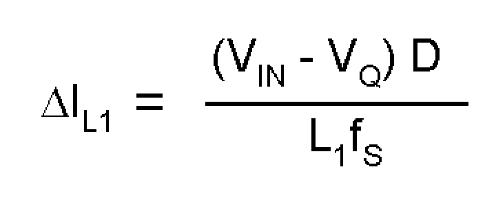
is the ripple voltage across the SEPIC capacitor, and

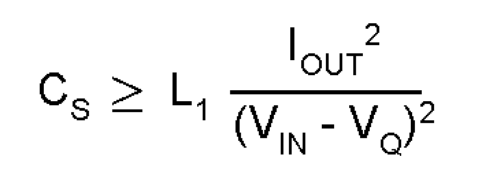
is the ripple current through the inductor L1. The energy balance equation can be solved using Equation 53 to provide a minimum value for CS.
