SNVS372G August 2005 – October 2016 LM4132 , LM4132-Q1
PRODUCTION DATA.
- 1 Features
- 2 Applications
- 3 Description
- 4 Revision History
- 5 Pin Configuration and Functions
-
6 Specifications
- 6.1 Absolute Maximum Ratings
- 6.2 ESD Ratings
- 6.3 Recommended Operating Conditions
- 6.4 Thermal Information
- 6.5 Electrical Characteristics LM4132-1.8 (VOUT = 1.8 V)
- 6.6 Electrical Characteristics LM4132-2 (VOUT = 2.048 V)
- 6.7 Electrical Characteristics LM4132-2.5 (VOUT = 2.5 V)
- 6.8 Electrical Characteristics LM4132-3 (VOUT = 3 V)
- 6.9 Electrical Characteristics LM4132-3.3 (VOUT = 3.3 V)
- 6.10 Electrical Characteristics LM4132-3.3-Q1(VOUT = 3.3 V)
- 6.11 Electrical Characteristics LM4132-4.1 (VOUT = 4.096 V)
- 6.12 Typical Characteristics
- 7 Detailed Description
- 8 Applications and Implementation
- 9 Power Supply Recommendations
- 10Layout
- 11Device and Documentation Support
- 12Mechanical, Packaging, and Orderable Information
7 Detailed Description
7.1 Overview
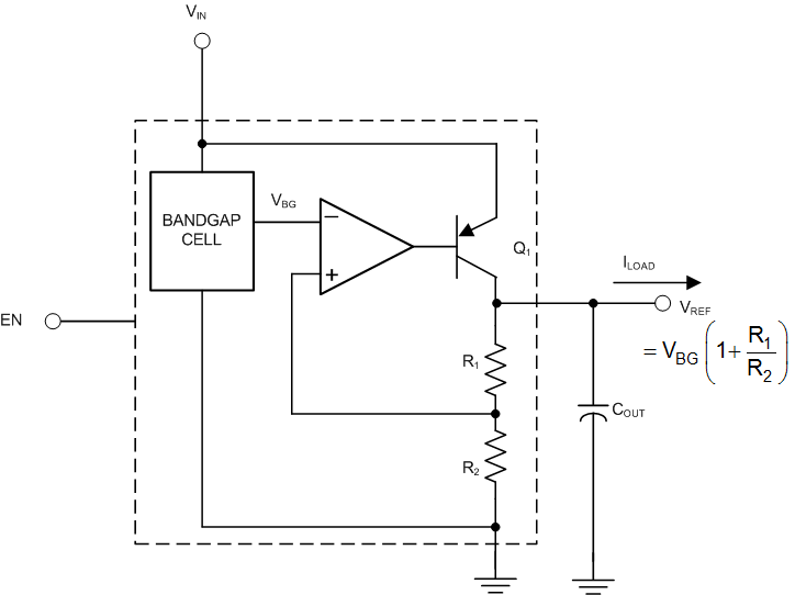
The LM4132 device is a precision band-gap voltage reference available in 6 different voltages with 20-mA current source capability. This series reference can operate with input voltages from VREF + 400 mV to 5.5 V while consuming 60-µA (typical) supply current. In shutdown mode, current drops to 3 µA (typical). The LM4132 is available in five grades from A and E.
The best grade devices (A) have an initial accuracy of 0.05% with a specified tempco of 10 ppm/°C from –40°C to 125°C. The grade devices (E) have an initial accuracy of 0.5% with specified tempco of 30 ppm/°C from –40°C to 125°C.
7.2 Functional Block Diagram

7.3 Feature Description
The LM4132 can be remotely operated by applying an EN voltage between 65% of VIN, and VIN. The LM4312 can be remotely disabled by applying an EN voltage between 0 V to 35% of VIN. The EN pin can also be strapped to VIN, so VREF is active when VIN is applied.
7.3.1 Short Circuited Output
The LM4132 features indefinite short-circuit protection. This protection limits the output current to 75 mA when the output is shorted to ground.
7.3.2 Turnon Time
Turnon time is defined as the time taken for the output voltage to rise to 90% of the preset value. The turnon time depends on the load. The turnon time is typically 33.2 µs when driving a 1-µF load and 78.8 µs when driving a 10-µF load. Some users may experience an extended turnon time (up to 10 ms) under brownout conditions and low temperatures (–40°C).
7.3.3 Thermal Hysteresis
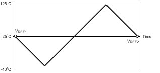
Thermal hysteresis is defined as the change in output voltage at 25ºC after some deviation from 25ºC. This is to say that thermal hysteresis is the difference in output voltage between two points in a given temperature profile. An illustrative temperature profile is shown in Figure 47.
 Figure 47. Temperature Profile
This may be expressed analytically by Equation 1:

where
- VHYS = Thermal hysteresis expressed in ppm
- VREF = Nominal preset output voltage
- VREF1 = VREF before temperature fluctuation
- VREF2 = VREF after temperature fluctuation
- The LM4132 features a low thermal hysteresis of 75 ppm (typical) from –40°C to 125°C after 8 temperature cycles.
7.4 Device Functional Modes
Table 1 describes the functional modes of the LM4132.
Table 1. Enable Pin Mode Summary
| ENABLE PIN CONNECTION | LOGIC STATE | DESCRIPTION |
|---|---|---|
| EN = VIN | 1 | Normal operation — LM4132 starts up. |
| EN = GND | 0 | The LM4312 is in shutdown mode. |