JAJSOF6 April 2022 LM5013-Q1
PRODUCTION DATA
- 1 特長
- 2 アプリケーション
- 3 概要
- 4 Revision History
- 5 Pin Configuration and Functions
- 6 Specifications
-
7 Detailed Description
- 7.1 Overview
- 7.2 Functional Block Diagram
- 7.3
Feature Description
- 7.3.1 Control Architecture
- 7.3.2 Internal VCC Regulator and Bootstrap Capacitor
- 7.3.3 Regulation Comparator
- 7.3.4 Internal Soft Start
- 7.3.5 On-Time Generator
- 7.3.6 Current Limit
- 7.3.7 N-Channel Buck Switch and Driver
- 7.3.8 Schottky Diode Selection
- 7.3.9 Enable/Undervoltage Lockout (EN/UVLO)
- 7.3.10 Power Good (PGOOD)
- 7.3.11 Thermal Protection
- 7.4 Device Functional Modes
- 8 Application and Implementation
- 9 Power Supply Recommendations
- 10Layout
- 11Device and Documentation Support
- 12Mechanical, Packaging, and Orderable Information
パッケージ・オプション
メカニカル・データ(パッケージ|ピン)
- DDA|8
サーマルパッド・メカニカル・データ
- DDA|8
発注情報
8.2.2.7 Type 3 Ripple Network
A Type 3 ripple generation network uses an RC filter consisting of RA and CA across SW and VOUT to generate a triangular ramp that is in-phase with the inductor current. This triangular ramp is then AC-coupled into the feedback node using capacitor CB as shown in Figure 8-1. Type 3 ripple injection is suited for applications where low output voltage ripple is crucial.
Use Equation 16 and Equation 17 to calculate RA and CA to provide the required ripple amplitude at the FB pin.
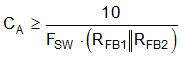
For the feedback resistors RFBT = 453 kΩ and RFBB = 49.9 kΩ values shown in Figure 8-1, Equation 16 dictates a minimum CA of 742 pF. In this design, a 3300-pF capacitance is chosen. This is done to keep RA within practical limits between 100 kΩ and 1 MΩ when using Equation 17.
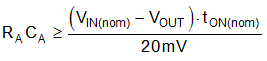
Based on CA set at 3.3 nF, RA is calculated to be 453 kΩ to provide a 20-mV ripple voltage at FB. The general recommendation for a Type 3 network is to calculate RA and CA to get 20 mV of ripple at typical operating conditions. A smaller RA can be required to operate below nominal 48-V input.
While the amplitude of the generated ripple does not affect the output voltage ripple, it impacts the output regulation as it reflects as a DC error of approximately half the amplitude of the generated ripple. For example, a converter circuit with Type 3 network that generates a 40-mV ripple voltage at the feedback node has approximately 10-mV worse load regulation scaled up through the FB divider to VOUT than the same circuit that generates a 20-mV ripple at FB. Use Equation 18 to calculate the coupling capacitance, CB.
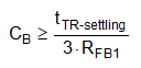
where
- tTR-settling is the desired load transient response settling time.
CB calculates to 56 pF based on a 75-µs settling time. This value avoids excessive coupling capacitor discharge by the feedback resistors during sleep intervals when operating at light loads. To avoid capacitance fall-off with DC bias, use a C0G or NP0 dielectric capacitor for CB.