JAJSOF6 April   2022 LM5013-Q1

PRODUCTION DATA  

  1. 特長
  2. アプリケーション
  3. 概要
  4. Revision History
  5. Pin Configuration and Functions
  6. Specifications
    1. 6.1 Absolute Maximum Ratings
    2. 6.2 ESD Ratings
    3. 6.3 Recommended Operating Conditions
    4. 6.4 Thermal Information
    5. 6.5 Electrical Characteristics
    6. 6.6 Typical Characteristics
  7. Detailed Description
    1. 7.1 Overview
    2. 7.2 Functional Block Diagram
    3. 7.3 Feature Description
      1. 7.3.1  Control Architecture
      2. 7.3.2  Internal VCC Regulator and Bootstrap Capacitor
      3. 7.3.3  Regulation Comparator
      4. 7.3.4  Internal Soft Start
      5. 7.3.5  On-Time Generator
      6. 7.3.6  Current Limit
      7. 7.3.7  N-Channel Buck Switch and Driver
      8. 7.3.8  Schottky Diode Selection
      9. 7.3.9  Enable/Undervoltage Lockout (EN/UVLO)
      10. 7.3.10 Power Good (PGOOD)
      11. 7.3.11 Thermal Protection
    4. 7.4 Device Functional Modes
      1. 7.4.1 Shutdown Mode
      2. 7.4.2 Standby Mode
      3. 7.4.3 Active Mode
      4. 7.4.4 Sleep Mode
  8. Application and Implementation
    1. 8.1 Application Information
    2. 8.2 Typical Application
      1. 8.2.1 Design Requirements
      2. 8.2.2 Detailed Design Procedure
        1. 8.2.2.1 Custom Design With WEBENCH® Tools
        2. 8.2.2.2 Switching Frequency (RRON)
        3. 8.2.2.3 Buck Inductor (LO)
        4. 8.2.2.4 Schottky Diode (DSW)
        5. 8.2.2.5 Output Capacitor (COUT)
        6. 8.2.2.6 Input Capacitor (CIN)
        7. 8.2.2.7 Type 3 Ripple Network
      3. 8.2.3 Application Curves
  9. Power Supply Recommendations
  10. 10Layout
    1. 10.1 Layout Guidelines
      1. 10.1.1 Compact PCB Layout for EMI Reduction
      2. 10.1.2 Feedback Resistors
    2. 10.2 Layout Example
      1. 10.2.1 Thermal Considerations
  11. 11Device and Documentation Support
    1. 11.1 Device Support
      1. 11.1.1 Third-Party Products Disclaimer
      2. 11.1.2 Development Support
        1. 11.1.2.1 Custom Design With WEBENCH® Tools
    2. 11.2 Documentation Support
      1. 11.2.1 Related Documentation
    3. 11.3 Receiving Notification of Documentation Updates
    4. 11.4 サポート・リソース
    5. 11.5 Trademarks
    6. 11.6 Electrostatic Discharge Caution
    7. 11.7 Glossary
  12. 12Mechanical, Packaging, and Orderable Information

パッケージ・オプション

メカニカル・データ(パッケージ|ピン)
サーマルパッド・メカニカル・データ
発注情報

Output Capacitor (COUT)

Select a ceramic output capacitor to limit the capacitive voltage ripple at the converter output. This is the sinusoidal ripple voltage that is generated from the triangular inductor current ripple flowing into and out of the capacitor. Select an output capacitance using Equation 13 to limit the voltage ripple component to 0.5% of the output voltage.

Equation 13. GUID-BEFFC5DD-5882-44A8-BF01-D034A4DCC556-low.gif

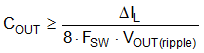
Substituting ΔIL(nom) of 1.36 A gives COUT greater than 10 μF. Considering the voltage coefficients of ceramic capacitors, a 22-µF, 25-V rated capacitor with X7R dielectric is selected.