JAJSK70B october 2020 – august 2023 LM5157-Q1 , LM51571-Q1
PRODUCTION DATA
- 1
- 1 特長
- 2 アプリケーション
- 3 概要
- 4 Revision History
- 5 概要 (続き)
- 6 Device Comparison Table
- 7 Pin Configuration and Functions
- 8 Specifications
-
9 Detailed Description
- 9.1 Overview
- 9.2 Functional Block Diagram
- 9.3
Feature Description
- 9.3.1 Line Undervoltage Lockout (UVLO/SYNC/EN Pin)
- 9.3.2 High Voltage VCC Regulator (BIAS, VCC Pin)
- 9.3.3 Soft Start (SS Pin)
- 9.3.4 Switching Frequency (RT Pin)
- 9.3.5 Dual Random Spread Spectrum – DRSS (MODE Pin)
- 9.3.6 Clock Synchronization (UVLO/SYNC/EN Pin)
- 9.3.7 Current Sense and Slope Compensation
- 9.3.8 Current Limit and Minimum On Time
- 9.3.9 Feedback and Error Amplifier (FB, COMP Pin)
- 9.3.10 Power-Good Indicator (PGOOD Pin)
- 9.3.11 Hiccup Mode Overload Protection (MODE Pin)
- 9.3.12 Maximum Duty Cycle Limit and Minimum Input Supply Voltage
- 9.3.13 Internal MOSFET (SW Pin)
- 9.3.14 Overvoltage Protection (OVP)
- 9.3.15 Thermal Shutdown (TSD)
- 9.4 Device Functional Modes
- 10Application and Implementation
- 11Power Supply Recommendations
- 12Layout
- 13Device and Documentation Support
- 14Mechanical, Packaging, and Orderable Information
パッケージ・オプション
メカニカル・データ(パッケージ|ピン)
- RTE|16
サーマルパッド・メカニカル・データ
- RTE|16
発注情報
10.3 System Examples
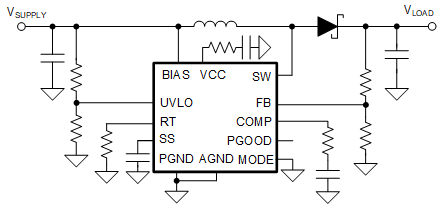 Figure 10-3 Typical Boost
Application
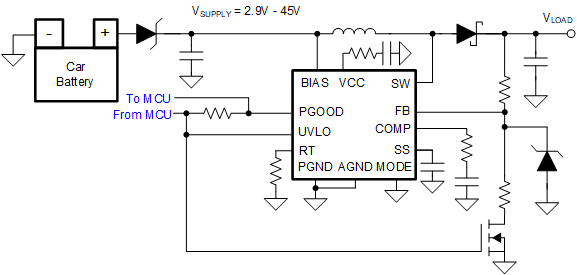 Figure 10-4 Typical Start-Stop
Application
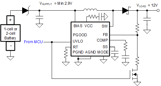 Figure 10-5 Emergency-Call/Boost
On-Demand/Portable Speaker
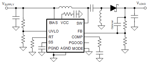 Figure 10-6 Typical SEPIC
Application
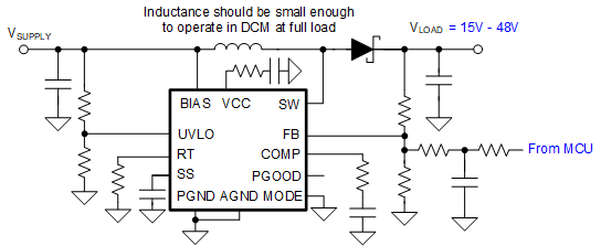 Figure 10-7 LiDAR Bias Supply 1 (DCM
Operation)
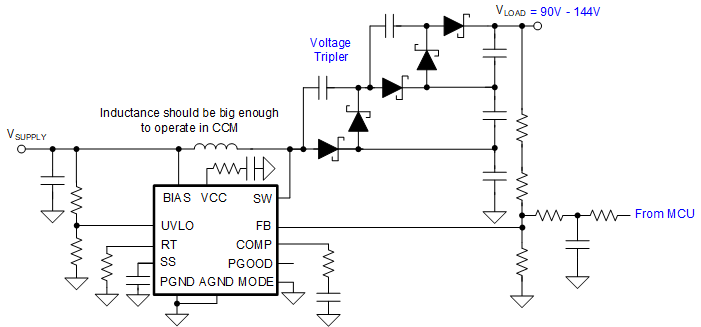 Figure 10-8 LiDAR Bias Supply 2 (CCM
Operation)
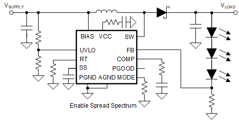 Figure 10-9 Low-Cost Single String LED
Driver
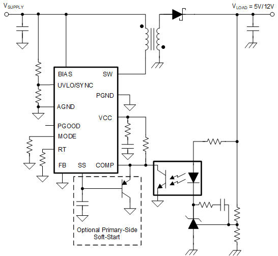 Figure 10-10 Secondary-Side Regulated
Isolated Flyback
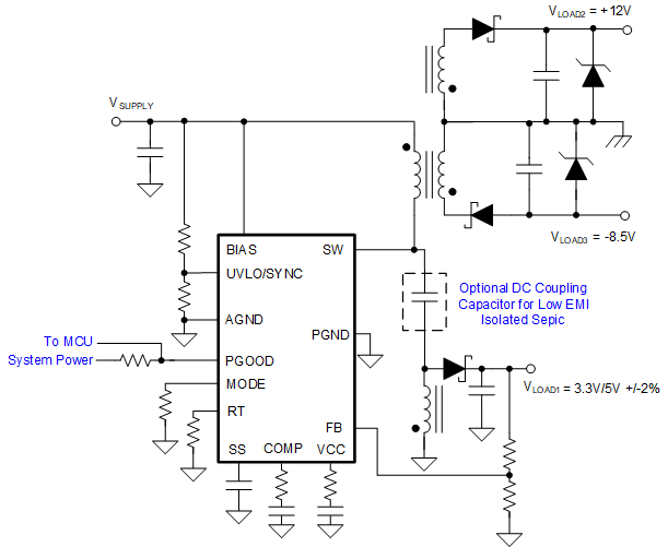 Figure 10-11 Primary-Side Regulated
Multiple-Output Isolated Flyback/Isolated SEPIC
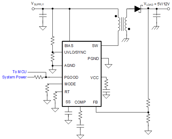 Figure 10-12 Typical Non-Isolated
Flyback