JAJSI29 October 2019 LM5163
PRODUCTION DATA.
- 1 特長
- 2 アプリケーション
- 3 概要
- 4 改訂履歴
- 5 概要(続き)
- 6 Pin Configuration and Functions
- 7 Specifications
-
8 Detailed Description
- 8.1 Overview
- 8.2 Functional Block Diagram
- 8.3
Feature Description
- 8.3.1 Control Architecture
- 8.3.2 Internal VCC Regulator and Bootstrap Capacitor
- 8.3.3 Regulation Comparator
- 8.3.4 Internal Soft Start
- 8.3.5 On-Time Generator
- 8.3.6 Current Limit
- 8.3.7 N-Channel Buck Switch and Driver
- 8.3.8 Synchronous Rectifier
- 8.3.9 Enable/Undervoltage Lockout (EN/UVLO)
- 8.3.10 Power Good (PGOOD)
- 8.3.11 Thermal Protection
- 8.4 Device Functional Modes
- 9 Application and Implementation
- 10Power Supply Recommendations
- 11Layout
- 12デバイスおよびドキュメントのサポート
- 13メカニカル、パッケージ、および注文情報
7.6 Typical Characteristics
At TA = 25°C, VOUT = 12 V, LO = 120 µH, RRON = 105 kΩ, unless otherwise specified. Figure 1. Conversion Efficiency (Log Scale)
  Figure 3. VIN Shutdown and Sleep Supply Current versus Temperature
  Figure 5. VIN Active Current versus Temperature
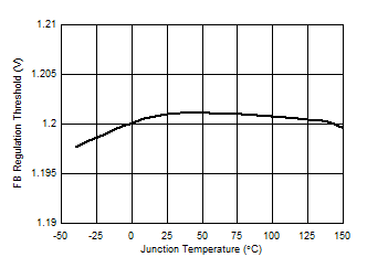
  Figure 7. Feedback Comparator Threshold versus Temperature
  Figure 9. Peak and Valley Current Limit versus Temperature
  Figure 2. Conversion Efficiency (Linear Scale)
  Figure 4. VIN Shutdown and Sleep Supply Current versus Input Voltage
  Figure 6. VIN Active Current versus Input Voltage
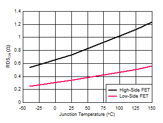
  Figure 8. MOSFETs On-State Resistance versus Temperature
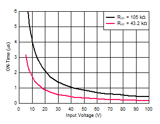
  Figure 10. COT On-Time versus VIN