JAJSFS7B July 2018 – February 2019 LM5180-Q1
ADVANCE INFORMATION for pre-production products; subject to change without notice.
- 1 特長
- 2 アプリケーション
- 3 概要
- 4 改訂履歴
- 5 概要(続き)
- 6 Pin Configuration and Functions
- 7 Specifications
-
8 Detailed Description
- 8.1 Overview
- 8.2 Functional Block Diagram
- 8.3
Feature Description
- 8.3.1 Integrated Power MOSFET
- 8.3.2 PSR Flyback Modes of Operation
- 8.3.3 Setting the Output Voltage
- 8.3.4 Control Loop Error Amplifier
- 8.3.5 Precision Enable
- 8.3.6 Configurable Soft Start
- 8.3.7 External Bias Supply
- 8.3.8 Minimum On-Time and Off-Time
- 8.3.9 Overcurrent Protection
- 8.3.10 Thermal Shutdown
- 8.4 Device Functional Modes
-
9 Application and Implementation
- 9.1 Application Information
- 9.2
Typical Applications
- 9.2.1
Design 1: Wide VIN, Low IQ PSR Flyback Converter Rated at 5 V, 1 A
- 9.2.1.1 Design Requirements
- 9.2.1.2
Detailed Design Procedure
- 9.2.1.2.1 Custom Design With WEBENCH® Tools
- 9.2.1.2.2 Custom Design With Excel Quickstart Tool
- 9.2.1.2.3 Flyback Transformer – T1
- 9.2.1.2.4 Flyback Diode – DFLY
- 9.2.1.2.5 Clamp Circuit – DF, DCLAMP
- 9.2.1.2.6 Output Capacitor – COUT
- 9.2.1.2.7 Input Capacitor – CIN
- 9.2.1.2.8 Feedback Resistor – RFB
- 9.2.1.2.9 Thermal Compensation Resistor – RTC
- 9.2.1.2.10 UVLO Resistors – RUV1, RUV2
- 9.2.1.2.11 Soft-Start Capacitor – CSS
- 9.2.1.3 Application Curves
- 9.2.2 Design 2: PSR Flyback Converter With Dual Outputs of 15 V and –7.7 V at 200 mA
- 9.2.3 Design 3: PSR Flyback Converter With Stacked Dual Outputs of 24 V and 5 V
- 9.2.1
Design 1: Wide VIN, Low IQ PSR Flyback Converter Rated at 5 V, 1 A
- 10Power Supply Recommendations
- 11Layout
- 12デバイスおよびドキュメントのサポート
- 13メカニカル、パッケージ、および注文情報
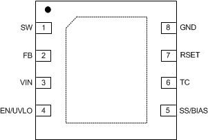
6 Pin Configuration and Functions
NGU Package
8-Pin WSON With Wettable Flanks
Top View

Pin Functions
| PIN | I/O(1) | DESCRIPTION | |
|---|---|---|---|
| NO. | NAME | ||
| 1 | SW | P | Switch node that is internally connected to the drain of the N-channel power MOSFET. Connect to the primary-side switching terminal of the flyback transformer. |
| 2 | FB | I | Primary side feedback pin. Connect a resistor from FB to SW. The ratio of the FB resistor to the resistor at the RSET pin sets the output voltage. |
| 3 | VIN | P/I | Input supply connection. Source for internal bias regulators and input voltage sensing pin. Connect directly to the input supply of the converter with short, low impedance paths. |
| 4 | EN/UVLO | I | Enable input and undervoltage lockout (UVLO) programming pin. If the EN/UVLO voltage is below 1.1 V, the converter is in shutdown mode with all functions disabled. If the EN/UVLO voltage is greater than 1.1 V and below 1.5 V, the converter is in standby mode with the internal regulator operational and no switching. If the EN/UVLO voltage is above 1.5 V, the start-up sequence begins. |
| 5 | SS/BIAS | I | Soft-start or bias input. Connect a capacitor from SS/BIAS to GND to adjust the output start-up time and input inrush current. If SS/BIAS is left open, the internal 6-ms soft-start timer is activated. Connect an auxiliary winding through a low leakage diode to SS/BIAS to supply bias to the internal voltage regulator and enable internal soft start. |
| 6 | TC | I | Temperature compensation pin. Tie a resistor from TC to RSET to compensate for the temperature coefficient of the forward voltage drop of the secondary diode, thus improving regulation at the secondary-side output. |
| 7 | RSET | I | Reference resistor tied to GND to set the reference current for FB. Connect a 12.1-kΩ resistor from RSET to GND. |
| 8 | GND | G | Analog and power ground. Ground connection of internal control circuits and power MOSFET. |
(1) P = Power, G = Ground, I = Input, O = Output.