JAJSI34G February 2019 – September 2022 LM63615-Q1 , LM63625-Q1
PRODUCTION DATA
- 1 特長
- 2 アプリケーション
- 3 概要
- 4 Revision History
- 5 Device Comparison Table
- 6 Pin Configuration and Functions
- 7 Specifications
- 8 Detailed Description
- 9 Application and Implementation
- 10Power Supply Recommendations
- 11Layout
- 12Device and Documentation Support
- 13Mechanical, Packaging, and Orderable Information
パッケージ・オプション
メカニカル・データ(パッケージ|ピン)
サーマルパッド・メカニカル・データ
発注情報
9.2.2.3 Inductor Selection
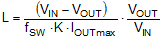
The parameters for selecting the inductor are the inductance and saturation current. The inductance is based on the desired peak-to-peak ripple current and is normally chosen to be in the range of 20% to 40% of the maximum output current. Experience shows that the best value for inductor ripple current is 30% of the maximum load current. Larger values of ripple current can restrict the maximum output current, before current limit is reached. This trade-off can be examined with the help of Equation 3 and the ensured current limits found in Section 7. Smaller values of ripple current reduce the SNR of the current mode controller and can lead to increased jitter in the duty cycle. Both the inductor and switching frequency tolerance have an impact on the selection of ripple current, and, therefore, inductor value. Use the maximum device current when calculating the ripple current for applications with much smaller maximum load than the maximum available from the device. The ratio of inductor ripple current over maximum output current is designated as K in the following equations. Equation 7 can be used to determine the value of inductance. K = 0.2 was chosen for this example and L = 2.8 µH inductance was found. A standard value of 2.2 µH was selected. This gives a new K = 0.25.
Ideally, the saturation current rating of the inductor is at least as large as the high-side switch current limit, ISC (see Section 7). This ensures that the inductor does not saturate even during a short circuit on the output. When the inductor core material saturates, the inductance falls to a very low value, causing the inductor current to rise very rapidly. Although the valley current limit, ILIMIT, is designed to reduce the risk of current run-away, a saturated inductor can cause the current to rise to high values very rapidly. This can lead to component damage. Do not allow the inductor to saturate. Inductors with a ferrite core material have very hard saturation characteristics, but usually have lower core losses than powdered iron cores. Powered iron cores exhibit a soft saturation, allowing some relaxation in the current rating of the inductor. However, they have more core losses at frequencies above about 1 MHz. In any case, the inductor saturation current must not be less than the maximum peak inductor current at full load.
To avoid subharmonic oscillation, the inductance value must not be less than that given in Equation 8. The maximum inductance is limited by the minimum current ripple required for the current mode control to perform correctly. As a rule-of-thumb, the minimum inductor ripple current must be no less than about 10% of the device maximum rated current under nominal conditions.

where
- M = 0.42 for 2.5 A device
- M = 0.69 for 1.5 A device