JAJSFL6D April   2016  – June 2018 LMH1226

PRODUCTION DATA.  

  1. 特長
  2. アプリケーション
  3. 概要
    1.     Device Images
      1.      ブロック概略図
  4. 改訂履歴
  5. Pin Configuration and Functions
    1.     Pin Functions
  6. Specifications
    1. 6.1 Absolute Maximum Ratings
    2. 6.2 ESD Ratings
    3. 6.3 Recommended Operating Conditions
    4. 6.4 Thermal Information
    5. 6.5 Electrical Characteristics
    6. 6.6 Recommended SMBus Interface AC Timing Specifications
    7. 6.7 Serial Parallel Interface (SPI) AC Timing Specifications
    8. 6.8 Typical Characteristics
  7. Detailed Description
    1. 7.1 Overview
    2. 7.2 Functional Block Diagram
    3. 7.3 Feature Description
      1. 7.3.1 4-Level Input Configuration Pins
      2. 7.3.2 Input Carrier Detect
      3. 7.3.3 Continuous Time Linear Equalizer (CTLE)
        1. 7.3.3.1 Adaptive PCB Trace Equalizer (IN1±)
      4. 7.3.4 Input-Output Mux Selection
      5. 7.3.5 Clock and Data Recovery (CDR) Reclocker
      6. 7.3.6 Internal Eye Opening Monitor (EOM)
      7. 7.3.7 Output Function Control
      8. 7.3.8 Output Driver Amplitude and De-Emphasis Control
      9. 7.3.9 Status Indicators and Interrupts
        1. 7.3.9.1 LOCK_N (Lock Indicator)
        2. 7.3.9.2 CD_N (Carrier Detect)
        3. 7.3.9.3 INT_N (Interrupt)
    4. 7.4 Device Functional Modes
      1. 7.4.1 System Management Bus (SMBus) Mode
        1. 7.4.1.1 SMBus Read and Write Transactions
          1. 7.4.1.1.1 SMBus Write Operation Format
          2. 7.4.1.1.2 SMBus Read Operation Format
      2. 7.4.2 Serial Peripheral Interface (SPI) Mode
        1. 7.4.2.1 SPI Read and Write Transactions
          1. 7.4.2.1.1 SPI Write Transaction Format
          2. 7.4.2.1.2 SPI Read Transaction Format
        2. 7.4.2.2 SPI Daisy Chain
    5. 7.5 LMH1226 Register Map
      1. 7.5.1 Share Register Page
      2. 7.5.2 CTLE/CDR Register Page
      3. 7.5.3 Drivers Register Page
  8. Application and Implementation
    1. 8.1 Application Information
      1. 8.1.1 General Guidance for SMPTE and 10 GbE Applications
      2. 8.1.2 LMH1219 and LMH1226 Compatibility
    2. 8.2 Typical Application
      1. 8.2.1 Design Requirements
      2. 8.2.2 Detailed Design Procedure
      3. 8.2.3 Recommended VOD and DEM Register Settings
      4. 8.2.4 Application Performance Plots
  9. Power Supply Recommendations
  10. 10Layout
    1. 10.1 PCB Layout Guidelines
    2. 10.2 Layout Example
  11. 11デバイスおよびドキュメントのサポート
    1. 11.1 ドキュメントの更新通知を受け取る方法
    2. 11.2 コミュニティ・リソース
    3. 11.3 商標
    4. 11.4 静電気放電に関する注意事項
    5. 11.5 Glossary
  12. 12メカニカル、パッケージ、および注文情報

パッケージ・オプション

メカニカル・データ(パッケージ|ピン)
サーマルパッド・メカニカル・データ
発注情報

SPI Daisy Chain

The LMH1226 supports SPI daisy-chaining among multiple devices, as shown in Figure 20.
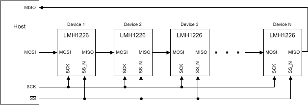
LMH1226 daisy_chain_configuration_snls517.gifFigure 20. Daisy-Chain Configuration

Each LMH1226 device is directly connected to the SCK and SS_N pins of the host. The first LMH1226 device in the chain is connected to the host’s MOSI pin, and the last device in the chain is connected to the host’s MISO pin. The MOSI pin of each intermediate LMH1226 device in the chain is connected to the MISO pin of the previous LMH1226 device, thereby creating a serial shift register. In a daisy-chain configuration of N x LMH1226 devices, the host conceptually sees a shift register of length 17 x N for a basic SPI transaction, during which SS_N is asserted low for 17 x N clock cycles.