JAJSI19D October 2019 – January 2023 LMH32401
PRODUCTION DATA
- 1 特長
- 2 アプリケーション
- 3 概要
- 4 Revision History
- 5 Pin Configuration and Functions
-
6 Specifications
- 6.1 Absolute Maximum Ratings
- 6.2 ESD Ratings
- 6.3 Recommended Operating Conditions
- 6.4 Thermal Information
- 6.5 Electrical Characteristics: Gain = 2 kΩ
- 6.6 Electrical Characteristics: Gain = 20 kΩ
- 6.7 Electrical Characteristics: Both Gains
- 6.8 Electrical Characteristics: Logic Threshold and Switching Characteristics
- 6.9 Typical Characteristics
- 7 Detailed Description
- 8 Application and Implementation
- 9 Power Supply Recommendations
- 10Layout
- 11Device and Documentation Support
- 12Mechanical, Packaging, and Orderable Information
パッケージ・オプション
デバイスごとのパッケージ図は、PDF版データシートをご参照ください。
メカニカル・データ(パッケージ|ピン)
- RGT|16
- Y|0
サーマルパッド・メカニカル・データ
- RGT|16
発注情報
7.4.2 Power-Down Mode (Multiplexer Mode)
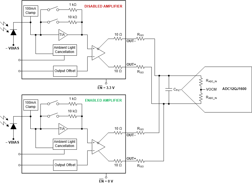
The LMH32401 device can be placed in low-power mode by setting EN high, which helps in saving system power. Enabling low-power mode puts the outputs of the internal amplifiers in the LMH32401 device, including the differential outputs, in a high-impedance state. #T5651494-2 shows how this device feature can further save board space and cost by eliminating the need for a discrete high-speed multiplexer, if a system consists of several photodiode and amplifier channels multiplexed to a single ADC channel. The disabled channel outputs are not an ideal open circuit so as the number of multiplexed channels increases the disabled channels begin to load the enabled channel. Multiplexing more than four channels in parallel degrades the performance of the enabled channel. When the amplifier is in its low-power mode, the clamp circuitry is still active thereby protecting the TIA input. The ambient light cancellation loop is disabled when the amplifier is placed in power-down mode. When the LMH32401 device is brought out of power-down operation the ambient light cancellation loop requires several time constants to settle. GUID-F7EAB361-04CF-4535-9EB1-C27793DE1F30.html#X8045 shows the low-frequency loop response which in turn determines the time constant needed for the loop to settle.
 Figure 7-3 Configuring Two LMH32401 Devices in Multiplexer Mode to
Drive a Single ADC