JAJSQ22J september 2011 – may 2023 LMK00301
PRODUCTION DATA
- 1
- 1 特長
- 2 アプリケーション
- 3 概要
- 4 Revision History
- 5 Device Comparison
- 6 Pin Configuration and Functions
- 7 Specifications
- 8 Parameter Measurement Information
- 9 Detailed Description
- 10Application and Implementation
- 11Power Supply Recommendations
- 12Layout
- 13Device and Documentation Support
- 14Mechanical, Packaging, and Orderable Information
パッケージ・オプション
メカニカル・データ(パッケージ|ピン)
- RHS|48
サーマルパッド・メカニカル・データ
- RHS|48
発注情報
10.2.2.1.3 Termination for Single-Ended Operation
A balun can be used with either LVDS or LVPECL drivers to convert the balanced, differential signal into an unbalanced, single-ended signal.
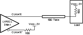
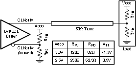
It is possible to use an LVPECL driver as one or two separate 800 mV p-p signals. When DC coupling one of the LMK00301 LVPECL driver of a CLKoutX/CLKoutX* pair, be sure to properly terminate the unused driver. When DC coupling on of the LMK00301 LVPECL drivers, the termination should be 50 Ω to Vcco - 2 V as shown in Figure 10-13. The Thevenin equivalent circuit is also a valid termination as shown in Figure 10-14 for Vcco = 3.3 V.
 Figure 10-13 Single-Ended LVPECL Operation, DC Coupling
 Figure 10-14 Single-Ended LVPECL Operation, DC Coupling, Thevenin Equivalent
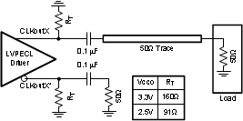
When AC coupling an LVPECL driver use a 160 Ω emitter resistor (or 91 Ω for Vcco = 2.5 V) to provide a DC path to ground and ensure a 50 Ω termination with the proper DC bias level for the receiver. The typical DC bias voltage for LVPECL receivers is 2 V. If the companion driver is not used, it should be terminated with either a proper AC or DC termination. This latter example of AC coupling a single-ended LVPECL signal can be used to measure single-ended LVPECL performance using a spectrum analyzer or phase noise analyzer. When using most RF test equipment no DC bias point (0 VDC) is required for safe and proper operation. The internal 50 Ω termination the test equipment correctly terminates the LVPECL driver being measured as shown in Figure 10-15. When using only one LVPECL driver of a CLKoutX/CLKoutX* pair, be sure to properly terminated the unused driver.
 Figure 10-15 Single-Ended LVPECL Operation, AC Coupling