SNOSAY9G September 2008 – February 2016 LMP2021 , LMP2022
PRODUCTION DATA.
- 1 Features
- 2 Applications
- 3 Description
- 4 Revision History
- 5 Pin Configuration and Functions SC-70 and VSSOP references from LMP2021 pinout descriptions
- 6 Specifications
- 7 Detailed Description
- 8 Application and Implementation
- 9 Power Supply Recommendations
- 10Layout
- 11Device and Documentation Support
- 12Mechanical, Packaging, and Orderable Information
7 Detailed Description
7.1 Overview
The LMP202x are single and dual precision operational amplifiers with ultra low offset voltage, ultra low offset voltage drift, and very low input voltage noise with no 1/f and extended supply voltage range. The LMP202x offer on chip EMI suppression circuitry which greatly enhances the performance of these precision amplifiers in the presence of radio frequency signals and other high frequency disturbances.
The LMP202x utilize proprietary auto zero techniques to measure and continuously correct the input offset error voltage. The LMP202x have a DC input offset voltage with a maximum value of ±5 μV and an input offset voltage drift maximum value of 0.02 µV/°C. The input voltage noise of the LMP202x is less than 11 nV/√Hz at a voltage gain of 1000 V/V and has no flicker noise component. This makes the LMP202x ideal for high accuracy, low frequency applications where lots of amplification is needed and the input signal has a very small amplitude.
The proprietary input offset correction circuitry enables the LMP202x to have superior CMRR and PSRR performances. The combination of an open loop voltage gain of 160 dB, CMRR of 142 dB, PSRR of 130 dB, along with the ultra low input offset voltage of only −0.4 µV, input offset voltage drift of only −0.004 µV/°C, and input voltage noise of only 260 nVPP at 0.1 Hz to 10 Hz make the LMP202x great choices for high gain transducer amplifiers, ADC buffer amplifiers, DAC I-V conversion, and other applications requiring precision and long-term stability. Other features are rail-to-rail output, low supply current of 1.1 mA per amplifier, and a gain-bandwidth product of 5 MHz.
The LMP202x have an extended supply voltage range of 2.2 V to 5.5 V, making them ideal for battery operated portable applications. The LMP2021 is offered in 5-pin SOT-23 and 8-pin SOIC packages. The LMP2022 is offered in 8-pin VSSOP and 8-Pin SOIC packages.
7.2 Functional Block Diagram

7.3 Feature Description
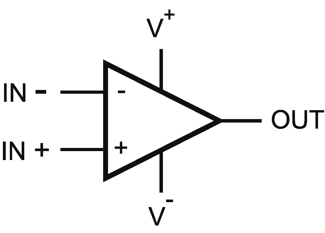
The amplifier's differential inputs consist of a non-inverting input (+IN) and an inverting input (–IN). The amplifier amplifies only the difference in voltage between the two inputs, which is called the differential input voltage. The output voltage of the op-amp Vout is given by Equation 1:
where AOL is the open-loop gain of the amplifier, typically around 100dB (100,000x, or 10uV per Volt).
7.4 Device Functional Modes
7.4.1 EMI Suppression
The near-ubiquity of cellular, Bluetooth, and Wi-Fi signals and the rapid rise of sensing systems incorporating wireless radios make electromagnetic interference (EMI) an evermore important design consideration for precision signal paths. Though RF signals lie outside the op amp band, RF carrier switching can modulate the DC offset of the op amp. Also some common RF modulation schemes can induce down-converted components. The added DC offset and the induced signals are amplified with the signal of interest and thus corrupt the measurement. The LMP202x use on chip filters to reject these unwanted RF signals at the inputs and power supply pins; thereby preserving the integrity of the precision signal path.
Twisted pair cabling and the active front-end’s common-mode rejection provide immunity against low frequency noise (i.e. 60 Hz or 50 Hz mains) but are ineffective against RF interference. Figure 46 displays this. Even a few centimeters of PCB trace and wiring for sensors located close to the amplifier can pick up significant 1 GHz RF. The integrated EMI filters of LMP202x reduce or eliminate external shielding and filtering requirements, thereby increasing system robustness. A larger EMIRR means more rejection of the RF interference. For more information on EMIRR, please refer to AN-1698 (Literature Number SNOA497).
7.4.2 Input Voltage Noise
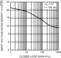
The input voltage noise density of the LMP202x has no 1/f corner, and its value depends on the feedback network used. This feature of the LMP202x differentiates this family from other products currently available from other vendors. In particular, the input voltage noise density decreases as the closed loop voltage gain of the LMP202x increases. The input voltage noise of the LMP202x is less than 11 nV/√Hz when the closed loop voltage gain of the op amp is 1000. Higher voltage gains are required for smaller input signals. When the input signal is smaller, a lower input voltage noise is quite advantageous and increases the signal to noise ratio.
Figure 35 shows the input voltage noise of the LMP202x as the closed loop gain increases.
 Figure 35. Input Voltage Noise Density decreases with Gain
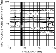
Figure 36 shows the input voltage noise density does not have the 1/f component.
 Figure 36. Input Voltage Noise Density with no 1/f
With smaller and smaller input signals and high precision applications with lower error budget, the reduced input voltage noise and no 1/f noise allow more flexibility in circuit design.