JAJSHL8B June 2012 – June 2019 LMR12015 , LMR12020
PRODUCTION DATA.
- 1 特長
- 2 アプリケーション
- 3 概要
- 4 改訂履歴
- 5 Pin Configuration and Functions
- 6 Specifications
- 7 Detailed Description
-
8 Application and Implementation
- 8.1 Application Information
- 8.2
Typical Application
- 8.2.1
Detailed Design Procedure
- 8.2.1.1 Custom Design With WEBENCH® Tools
- 8.2.1.2 Inductor Selection
- 8.2.1.3 Input Capacitor
- 8.2.1.4 Output Capacitor
- 8.2.1.5 Catch Diode
- 8.2.1.6 Boost Diode (Optional)
- 8.2.1.7 Boost Capacitor
- 8.2.1.8 Output Voltage
- 8.2.1.9 Feedforward Capacitor (Optional)
- 8.2.1.10
Calculating Efficiency and Junction Temperature
- 8.2.1.10.1 Schottky Diode Conduction Losses
- 8.2.1.10.2 Inductor Conduction Losses
- 8.2.1.10.3 MOSFET Conduction Losses
- 8.2.1.10.4 MOSFET Switching Losses
- 8.2.1.10.5 IC Quiescent Losses
- 8.2.1.10.6 MOSFET Driver Losses
- 8.2.1.10.7 Total Power Losses
- 8.2.1.10.8 Efficiency Calculation Example
- 8.2.1.10.9 Calculating the LMR2015/20 Junction Temperature
- 8.2.2 Application Curves
- 8.2.3 LMR12015/20 Circuit Examples
- 8.2.1
Detailed Design Procedure
- 9 Layout
- 10デバイスおよびドキュメントのサポート
- 11メカニカル、パッケージ、および注文情報
パッケージ・オプション
メカニカル・データ(パッケージ|ピン)
- DSC|10
サーマルパッド・メカニカル・データ
- DSC|10
発注情報
8.2.1.2 Inductor Selection
Inductor selection is critical to the performance of the LMR12015/20. The selection of the inductor affects stability, transient response and efficiency. A key factor in inductor selection is determining the ripple current (ΔiL) (see Figure 22).
The ripple current (ΔiL) is important in many ways.
First, by allowing more ripple current, lower inductance values can be used with a corresponding decrease in physical dimensions and improved transient response. On the other hand, allowing less ripple current will increase the maximum achievable load current and reduce the output voltage ripple (see Output Capacitor section for more details on calculating output voltage ripple). Increasing the maximum load current is achieved by ensuring that the peak inductor current (ILPK) never exceeds the minimum current limit of 2 A minimum (LMR12015) or 2.5 A minimum (LMR12020) .
Secondly, the slope of the ripple current affects the current control loop. The LMR12015/20 has a fixed slope corrective ramp. When the slope of the current ripple becomes significantly less than the converter’s corrective ramp (see ), the inductor pole will move from high frequencies to lower frequencies. This negates one advantage that peak current-mode control has over voltage-mode control, which is, a single low frequency pole in the power stage of the converter. This can reduce the phase margin, crossover frequency and potentially cause instability in the converter. Contrarily, when the slope of the ripple current becomes significantly greater than the converter’s corrective ramp, resonant peaking can occur in the control loop. This can also cause instability (sub-harmonic oscillation) in the converter. For the power supply designer this means that for lower switching frequencies the current ripple must be increased to keep the inductor pole well above crossover. It also means that for higher switching frequencies the current ripple must be decreased to avoid resonant peaking.
With all these factors, how is the desired ripple current selected? The ripple ratio (r) is defined as the ratio of inductor ripple current (ΔiL) to output current (IOUT), evaluated at maximum load:

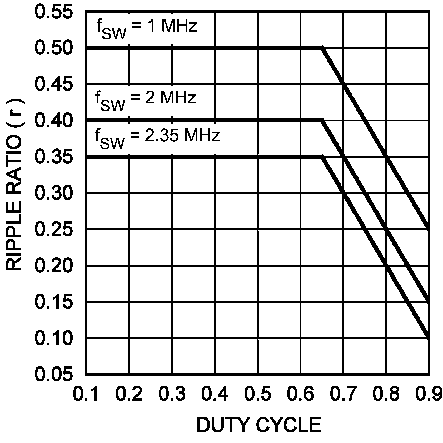
A good compromise between physical size, transient response and efficiency is achieved when we set the ripple ratio between 0.2 and 0.4. The recommended ripple ratio vs. duty cycle shown below (see Figure 27) is based upon this compromise and control loop optimizations. Note that this is just a guideline. See Application note AN-1197 AN-1197 Selecting Inductors for Buck Converters for further considerations.
 Figure 27. Recommended Ripple Ratio vs Duty Cycle
 The duty cycle (D) can be approximated quickly using the ratio of output voltage (VOUT) to input voltage (VIN):

Use the application's lowest input voltage to calculate the ripple ratio. The catch diode forward voltage drop (VD1) and the voltage drop across the internal NFET (VDS) must be included to calculate a more accurate duty cycle. Calculate D by using the following formula:

VDS can be approximated by:
The diode forward drop (VD1) can range from 0.3 V to 0.5 V depending on the quality of the diode. The lower VD1 is, the higher the operating efficiency of the converter.
Now that the ripple current or ripple ratio is determined, the required inductance is calculated by:

where
- DMIN is the duty cycle calculated with the maximum input voltage
- ƒSW is the switching frequency
- IOUT is the maximum output current of 2 A
Using IOUT = 2 A minimizes the inductor's physical size.