JAJSEV6E December 2015 – August 2020 LMR23630
PRODUCTION DATA
- 1 特長
- 2 アプリケーション
- 3 概要
- 4 Revision History
- 5 Device Comparison Table
- 6 Pin Configuration and Functions
- 7 Specifications
-
8 Detailed Description
- 8.1 Overview
- 8.2 Functional Block Diagram
- 8.3
Feature Description
- 8.3.1 Fixed Frequency Peak Current Mode Control
- 8.3.2 Adjustable Frequency
- 8.3.3 Adjustable Output Voltage
- 8.3.4 Enable/Sync
- 8.3.5 VCC, UVLO
- 8.3.6 Minimum ON-time, Minimum OFF-time and Frequency Foldback at Dropout Conditions
- 8.3.7 Power Good (PGOOD)
- 8.3.8 Internal Compensation and CFF
- 8.3.9 Bootstrap Voltage (BOOT)
- 8.3.10 Overcurrent and Short-Circuit Protection
- 8.3.11 Thermal Shutdown
- 8.4 Device Functional Modes
-
9 Application and Implementation
- 9.1 Application Information
- 9.2
Typical Applications
- 9.2.1 Design Requirements
- 9.2.2
Detailed Design Procedure
- 9.2.2.1 Custom Design With WEBENCH® Tools
- 9.2.2.2 Output Voltage Setpoint
- 9.2.2.3 Switching Frequency
- 9.2.2.4 Inductor Selection
- 9.2.2.5 Output Capacitor Selection
- 9.2.2.6 Feed-Forward Capacitor
- 9.2.2.7 Input Capacitor Selection
- 9.2.2.8 Bootstrap Capacitor Selection
- 9.2.2.9 VCC Capacitor Selection
- 9.2.2.10 Undervoltage Lockout Setpoint
- 9.2.3 Application Curves
- 10Power Supply Recommendations
- 11Layout
- 12Device and Documentation Support
- 13Mechanical, Packaging, and Orderable Information
パッケージ・オプション
デバイスごとのパッケージ図は、PDF版データシートをご参照ください。
メカニカル・データ(パッケージ|ピン)
- DDA|8
- DRR|12
サーマルパッド・メカニカル・データ
発注情報
9.2.2.5 Output Capacitor Selection
Choose the output capacitor(s), COUT, with care because it directly affects the steady-state output-voltage ripple, loop stability, and the voltage over/undershoot during load-current transients.
The output ripple is essentially composed of two parts. One is caused by the inductor current ripple going through the equivalent series resistance (ESR) of the output capacitors:

The other is caused by the inductor current ripple charging and discharging the output capacitors:
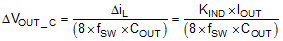
The two components in the voltage ripple are not in phase, so the actual peak-to-peak ripple is smaller than the sum of two peaks.
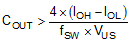
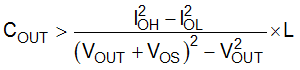
Output capacitance is usually limited by transient performance specifications if the system requires tight voltage regulation with presence of large current steps and fast slew rate. When a fast large load increase happens, output capacitors provide the required charge before the inductor current can slew up to the appropriate level. The control loop of the regulator usually needs four or more clock cycles to respond to the output voltage droop. The output capacitance must be large enough to supply the current difference for four clock cycles to maintain the output voltage within the specified range. Equation 17 shows the minimum output capacitance needed for specified output undershoot. When a sudden large load decrease happens, the output capacitors absorb energy stored in the inductor. which results in an output voltage overshoot. Equation 14 calculates the minimum capacitance required to keep the voltage overshoot within a specified range.
where
- IOL = Low level output current during load transient
- IOH = High level output current during load transient
- VUS = Target output voltage undershoot
- VOS = Target output voltage overshoot
For this design example, the target output ripple is 50 mV. Presuppose ΔVOUT_ESR = ΔVOUT_C = 50 mV, and chose KIND = 0.4. Equation 16 yields ESR no larger than 41.7 mΩ and Equation 17 yields COUT no smaller than 7.5 μF. For the target over/undershoot range of this design, VUS = VOS = 5% × VOUT = 250 mV. The COUT can be calculated to be no smaller than 108 μF and 28.5 μF by Equation 15 and Equation 17, respectively. Consider of derating, one 47-μF, 16-V and one 100-μF, 10-V ceramic capacitor with 5-mΩ ESR are used in parallel.