JAJSEV6E December 2015 – August 2020 LMR23630
PRODUCTION DATA
- 1 特長
- 2 アプリケーション
- 3 概要
- 4 Revision History
- 5 Device Comparison Table
- 6 Pin Configuration and Functions
- 7 Specifications
-
8 Detailed Description
- 8.1 Overview
- 8.2 Functional Block Diagram
- 8.3
Feature Description
- 8.3.1 Fixed Frequency Peak Current Mode Control
- 8.3.2 Adjustable Frequency
- 8.3.3 Adjustable Output Voltage
- 8.3.4 Enable/Sync
- 8.3.5 VCC, UVLO
- 8.3.6 Minimum ON-time, Minimum OFF-time and Frequency Foldback at Dropout Conditions
- 8.3.7 Power Good (PGOOD)
- 8.3.8 Internal Compensation and CFF
- 8.3.9 Bootstrap Voltage (BOOT)
- 8.3.10 Overcurrent and Short-Circuit Protection
- 8.3.11 Thermal Shutdown
- 8.4 Device Functional Modes
-
9 Application and Implementation
- 9.1 Application Information
- 9.2
Typical Applications
- 9.2.1 Design Requirements
- 9.2.2
Detailed Design Procedure
- 9.2.2.1 Custom Design With WEBENCH® Tools
- 9.2.2.2 Output Voltage Setpoint
- 9.2.2.3 Switching Frequency
- 9.2.2.4 Inductor Selection
- 9.2.2.5 Output Capacitor Selection
- 9.2.2.6 Feed-Forward Capacitor
- 9.2.2.7 Input Capacitor Selection
- 9.2.2.8 Bootstrap Capacitor Selection
- 9.2.2.9 VCC Capacitor Selection
- 9.2.2.10 Undervoltage Lockout Setpoint
- 9.2.3 Application Curves
- 10Power Supply Recommendations
- 11Layout
- 12Device and Documentation Support
- 13Mechanical, Packaging, and Orderable Information
パッケージ・オプション
デバイスごとのパッケージ図は、PDF版データシートをご参照ください。
メカニカル・データ(パッケージ|ピン)
- DDA|8
- DRR|12
サーマルパッド・メカニカル・データ
発注情報
8.3.2 Adjustable Frequency
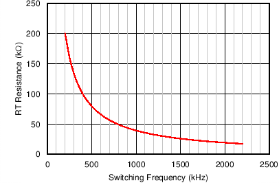
The switching frequency can be programmed for the adjustable-switching-frequency version of LMR23630 by the impedance RT from the RT pin to ground. The frequency is inversely proportional to the RT resistance. The RT pin can be left floating and the LMR23630 operates at 400-kHz default switching frequency. The RT pin is not designed to be shorted to ground. For a desired frequency, typical RT resistance can be found by Equation 1. Table 8-1 gives typical RT values for a given fSW.
Equation 1. RT(kΩ) = 40200 / fSW(kHz) – 0.6
 Figure 8-2 RT vs Frequency Curve
Table 8-1 Typical Frequency Setting RT Resistance
| fSW (kHz) | RT (kΩ) |
|---|---|
| 200 | 200 |
| 350 | 115 |
| 500 | 78.7 |
| 750 | 53.6 |
| 1000 | 39.2 |
| 1500 | 26.1 |
| 2000 | 19.6 |
| 2200 | 17.8 |