SNOSCY7 June 2014 LP2996A
PRODUCTION DATA.
- 1 Features
- 2 Applications
- 3 Description
- 4 Revision History
- 5 Pin Configuration and Functions
- 6 Specifications
- 7 Detailed Description
- 8 Applications and Implementation
- 9 Power Supply Recommendations
- 10Layout
- 11Device and Documentation Support
- 12Mechanical, Packaging, and Orderable Information
- 11Mechanical, Packaging, and Orderable Information
パッケージ・オプション
メカニカル・データ(パッケージ|ピン)
- DDA|8
サーマルパッド・メカニカル・データ
- DDA|8
発注情報
6 Specifications
6.1 Absolute Maximum Ratings (1)(2)
over operating free-air temperature range (unless otherwise noted)| MIN | MAX | UNIT | ||
|---|---|---|---|---|
| AVIN to GND | −0.3 | 6 | V | |
| PVIN to GND | –0.3 | AVIN | ||
| VDDQ(1) | −0.3 | 6 | V | |
| Junction Temperature | 150 | °C | ||
| Lead Temperature (Soldering, 10 sec) | 260 | °C |
(1) Stresses beyond those listed under absolute maximum ratings may cause permanent damage to the device. These are stress ratings only, and functional operation of the device at these or any other conditions beyond those indicated under recommended operating conditions is not implied. Exposure to absolute–maximum–rated conditions for extended periods may affect device reliability.
(2) If Military/Aerospace specified devices are required, please contact the Texas Instruments Sales Office/Distributors for availability and specifications.
6.2 Handling Ratings
| MIN | MAX | UNIT | |||
|---|---|---|---|---|---|
| Tstg | Storage temperature range | −65 | 150 | °C | |
| V(ESD) | Electrostatic discharge | Human body model (HBM), per ANSI/ESDA/JEDEC JS-001, all pins(1) | 1 | kV | |
(1) JEDEC document JEP155 states that 500-V HBM allows safe manufacturing with a standard ESD control process.
6.3 Recommended Operating Conditions
over operating free-air temperature range (unless otherwise noted)| MIN | NOM | MAX | UNIT | ||
|---|---|---|---|---|---|
| Junction Temp. Range(2) | 0 | 125 | °C | ||
| AVIN to GND | 2.2 | 5.5 | V | ||
| PVIN Supply Voltage | 0 | AVIN | |||
| SD Input Voltage | 0 | AVIN | |||
6.4 Thermal Information
| THERMAL METRIC(1)(2)(3) | SO PowerPAD-8 DDA | UNIT | |
|---|---|---|---|
| 8 PINS | |||
| RθJA | Junction-to-ambient thermal resistance | 56.5 | °C/W |
| RθJC(top) | Junction-to-case (top) thermal resistance | 65.1 | |
| RθJB | Junction-to-board thermal resistance | 36.5 | |
| ψJT | Junction-to-top characterization parameter | 15.9 | |
| ψJB | Junction-to-board characterization parameter | 36.5 | |
| RθJC(bot) | Junction-to-case (bottom) thermal resistance | 8.4 | |
(1) For more information about traditional and new thermal metrics, see the IC Package Thermal Metrics application report, SPRA953.
(2) The package thermal impedance is calculated in accordance with JESD 51-7
(3) Thermal Resistances were simulated on a 4 layer, JEDEC board.
6.5 Electrical Characteristics
Specifications are for TJ = 25°C and apply over the full Operating Temperature Range (TJ = 0°C to +125°C)(3). Unless otherwise specified, AVIN = PVIN = 2.5V, VDDQ = 2.5V(4).| PARAMETER | TEST CONDITIONS | MIN | TYP | MAX | UNIT | |
|---|---|---|---|---|---|---|
| VREF | VREF voltage (DDR I) | VIN = VDDQ = 2.3 V | 1.135 | 1.158 | 1.185 | V |
| VIN = VDDQ = 2.5 V | 1.235 | 1.258 | 1.285 | |||
| VIN = VDDQ = 2.7 V | 1.335 | 1.358 | 1.385 | |||
| VREF voltage (DDR II) | PVIN = VDDQ = 1.7 V | 0.837 | 0.860 | 0.887 | ||
| PVIN = VDDQ = 1.8 V | 0.887 | 0.910 | 0.937 | |||
| PVIN = VDDQ = 1.9 V | 0.936 | 0.959 | 0.986 | |||
| VREF Voltage (DDR III) | PVIN = VDDQ = 1.35V | 0.669 | 0.684 | 0.699 | ||
| PVIN = VDDQ = 1.5V | 0.743 | 0.758 | 0.773 | |||
| PVIN = VDDQ = 1.6V | 0.793 | 0.808 | 0.823 | |||
| ZVREF | VREF Output Impedance | IREF = –30 to +30 µA | 2.5 | kΩ | ||
| VTT | VTT Output Voltage (DDR I) (7) | IOUT = 0 A | V | |||
| VIN = VDDQ = 2.3 V | 1.120 | 1.159 | 1.190 | |||
| VIN = VDDQ = 2.5 V | 1.210 | 1.259 | 1.290 | |||
| VIN = VDDQ = 2.7 V | 1.320 | 1.359 | 1.390 | |||
| IOUT = +/– 1.5 A | ||||||
| VIN = VDDQ = 2.3 V | 1.125 | 1.159 | 1.190 | |||
| VIN = VDDQ = 2.5 V | 1.225 | 1.259 | 1.290 | |||
| VIN = VDDQ = 2.7 V | 1.325 | 1.359 | 1.390 | |||
| VTT Output Voltage (DDR II) (7) | IOUT = 0 A, AVIN = 2.5 V | V | ||||
| PVIN = VDDQ = 1.7 V | 0.822 | 0.856 | 0.887 | |||
| PVIN = VDDQ = 1.8 V | 0.874 | 0.908 | 0.939 | |||
| PVIN = VDDQ = 1.9 V | 0.923 | 0.957 | 0.988 | |||
| IOUT = +/– 0.5A, AVIN = 2.5 V | ||||||
| PVIN = VDDQ = 1.7 V | 0.820 | 0.856 | 0.890 | |||
| PVIN = VDDQ = 1.8 V | 0.870 | 0.908 | 0.940 | |||
| PVIN = VDDQ = 1.9 V | 0.920 | 0.957 | 0.990 | |||
| VTT Output Voltage (DDR III) (7) | IOUT = 0A, AVIN = 2.5 V | V | ||||
| PVIN = VDDQ = 1.35V | 0.656 | 0.677 | 0.698 | |||
| PVIN = VDDQ = 1.5 V | 0.731 | 0.752 | 0.773 | |||
| PVIN = VDDQ = 1.6 V | 0.781 | 0.802 | 0.823 | |||
| IOUT = +0.2A, AVIN = 2.5V PVIN = VDDQ = 1.35V |
0.667 | 0.688 | 0.710 | |||
| IOUT = -0.2A, AVIN = 2.5V PVIN = VDDQ = 1.35V |
0.641 | 0.673 | 0.694 | |||
| IOUT = +0.4 A, AVIN = 2.5 V PVIN = VDDQ = 1.5 V |
0.740 | 0.763 | 0.786 | |||
| IOUT = –0.4 A, AVIN = 2.5 V PVIN = VDDQ = 1.5 V |
0.731 | 0.752 | 0.773 | |||
| IOUT = +0.5A, AVIN = 2.5 V PVIN = VDDQ = 1.6 V |
0.790 | 0.813 | 0.836 | |||
| IOUT = -0.5 A, AVIN = 2.5 V PVIN = VDDQ = 1.6 V |
0.781 | 0.802 | 0.823 | |||
| VOSVtt | VTT Output Voltage Offset (VREF – VTT) for DDR I (7) | IOUT = 0 A | –30 | 0 | 30 | mV |
| IOUT = –1.5 A | –30 | 0 | 30 | |||
| IOUT = 1.5 A | –30 | 0 | 30 | |||
| VTT Output Voltage Offset (VREF – VTT) for DDR II (7) | IOUT = 0 A | –30 | 0 | 30 | ||
| IOUT = –0.5 A | –30 | 0 | 30 | |||
| IOUT = 0.5 A | –30 | 0 | 30 | |||
| VTT Output Voltage Offset (VREF – VTT) for DDR III (7) | IOUT = 0 A | –30 | 0 | 30 | ||
| IOUT = ±0.2 A | –30 | 0 | 30 | |||
| IOUT = ±0.4 A | –30 | 0 | 30 | |||
| IOUT = ±0.5 A | –30 | 0 | 30 | |||
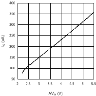
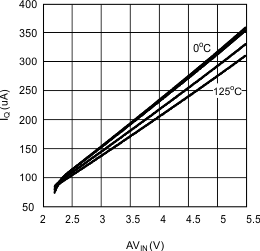
| IQ | Quiescent Current (5) | IOUT = 0 A | 320 | 500 | µA | |
| ZVDDQ | VDDQ Input Impedance | 100 | kΩ | |||
| ISD | Quiescent current in shutdown (5) | SD = 0 V | 115 | 150 | µA | |
| IQ_SD | Shutdown leakage current | SD = 0 V | 2 | 5 | ||
| VIH | Minimum Shutdown High Level | 1.9 | V | |||
| VIL | Maximum Shutdown Low Level | 0.8 | ||||
| Iv | VTT leakage current in shutdown | SD = 0 V VTT = 1.25 V |
1 | 10 | µA | |
| ISENSE | VSENSE Input current | 13 | nA | |||
| TSD | Thermal Shutdown (6) | 165 | °C | |||
| TSD_HYS | Thermal Shutdown Hysteresis | 10 | ||||
(1) Absolute maximum ratings indicate limits beyond which damage to the device may occur. Operating range indicates conditions for which the device is intended to be functional, but does not ensure specific performance limits. For ensured specifications and test conditions see Electrical Characteristics. The ensured specifications apply only for the test conditions listed. Some performance characteristics may degrade when the device is not operated under the listed test conditions.
(2) At elevated temperatures, devices must be derated based on thermal resistance.
(3) Limits are 100% production tested at 25°C. Limits over the operating temperature range are specified through correlation using Statistical Quality Control (SQC) methods. The limits are used to calculate Texas Instruments' Average Outgoing Quality Level (AOQL).
(4) VIN is defined as VIN = AVIN = PVIN.
(5) Quiescent current defined as the current flow into AVIN.
(6) The maximum allowable power dissipation is a function of the maximum junction temperature, TJ(MAX), the junction to ambient thermal resistance, θJA, and the ambient temperature, TA. Exceeding the maximum allowable power dissipation will cause excessive die temperature and the regulator will go into thermal shutdown.
(7) VTT load regulation is tested by using a 10 ms current pulse and measuring VTT.
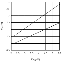
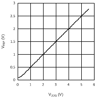
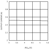
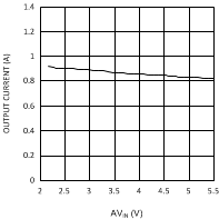
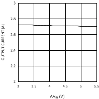
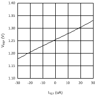
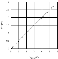
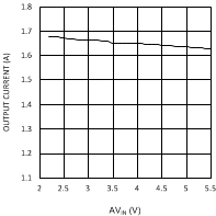
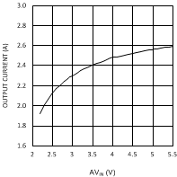
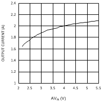
6.6 Typical Performance Characteristics
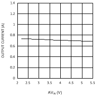
(VDDQ = 2.5 V, PVIN = 1.8 V)
(VDDQ = 2.5 V, PVIN = 3.3 V)
(VDDQ = 1.8 V, PVIN = 1.8 V)
(VDDQ = 1.8 V, PVIN = 3.3 V)
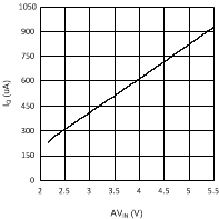
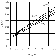
(VDDQ = 2.5 V, PVIN = 2.5 V)
(VDDQ = 2.5 V)
(VDDQ = 1.8 V)