JAJSCD5A August 2016 – August 2016 MSP430F6459-HIREL
PRODUCTION DATA.
- 1デバイスの概要
- 2改訂履歴
- 3Device Comparison
- 4Terminal Configuration and Functions
-
5Specifications
- 5.1 Absolute Maximum Ratings
- 5.2 ESD Ratings
- 5.3 Recommended Operating Conditions
- 5.4 Active Mode Supply Current Into VCC Excluding External Current
- 5.5 Low-Power Mode Supply Currents (Into VCC) Excluding External Current
- 5.6 Low-Power Mode With LCD Supply Currents (Into VCC) Excluding External Current
- 5.7 Schmitt-Trigger Inputs - General-Purpose I/O
- 5.8 Leakage Current - General-Purpose I/O
- 5.9 Outputs - General-Purpose I/O (Full Drive Strength)
- 5.10 Outputs - General-Purpose I/O (Reduced Drive Strength)
- 5.11 Thermal Resistance Characteristics for PZ Package
- 5.12 Typical Characteristics - Outputs, Reduced Drive Strength (PxDS.y = 0)
- 5.13 Typical Characteristics - Outputs, Full Drive Strength (PxDS.y = 1)
- 5.14 Timing and Switching Characteristics
-
6Detailed Description
- 6.1 Overview
- 6.2 CPU
- 6.3 Instruction Set
- 6.4 Operating Modes
- 6.5 Interrupt Vector Addresses
- 6.6 Memory Organization
- 6.7 Bootloader (BSL)
- 6.8 JTAG Operation
- 6.9 Flash Memory
- 6.10 Memory Integrity Detection (MID)
- 6.11 RAM
- 6.12 Backup RAM
- 6.13
Peripherals
- 6.13.1 Digital I/O
- 6.13.2 Port Mapping Controller
- 6.13.3 Oscillator and System Clock
- 6.13.4 Power-Management Module (PMM)
- 6.13.5 Hardware Multiplier (MPY)
- 6.13.6 Real-Time Clock (RTC_B)
- 6.13.7 Watchdog Timer (WDT_A)
- 6.13.8 System Module (SYS)
- 6.13.9 DMA Controller
- 6.13.10 Universal Serial Communication Interface (USCI)
- 6.13.11 Timer TA0
- 6.13.12 Timer TA1
- 6.13.13 Timer TA2
- 6.13.14 Timer TB0
- 6.13.15 Comparator_B
- 6.13.16 ADC12_A
- 6.13.17 DAC12_A
- 6.13.18 CRC16
- 6.13.19 Voltage Reference (REF) Module
- 6.13.20 LCD_B
- 6.13.21 LDO and PU Port
- 6.13.22 Embedded Emulation Module (EEM) (L Version)
- 6.13.23 Peripheral File Map
- 6.14
Input/Output Schematics
- 6.14.1 Port P1, P1.0 to P1.7, Input/Output With Schmitt Trigger
- 6.14.2 Port P2, P2.0 to P2.7, Input/Output With Schmitt Trigger
- 6.14.3 Port P3, P3.0 to P3.7, Input/Output With Schmitt Trigger
- 6.14.4 Port P4, P4.0 to P4.7, Input/Output With Schmitt Trigger
- 6.14.5 Port P5, P5.0 and P5.1, Input/Output With Schmitt Trigger
- 6.14.6 Port P5, P5.2 to P5.7, Input/Output With Schmitt Trigger
- 6.14.7 Port P6, P6.0 to P6.7, Input/Output With Schmitt Trigger
- 6.14.8 Port P7, P7.2, Input/Output With Schmitt Trigger
- 6.14.9 Port P7, P7.3, Input/Output With Schmitt Trigger
- 6.14.10 Port P7, P7.4 to P7.7, Input/Output With Schmitt Trigger
- 6.14.11 Port P8, P8.0 to P8.7, Input/Output With Schmitt Trigger
- 6.14.12 Port P9, P9.0 to P9.7, Input/Output With Schmitt Trigger
- 6.14.13 Port PU.0, PU.1 Ports
- 6.14.14 Port J, PJ.0 JTAG Pin TDO, Input/Output With Schmitt Trigger or Output
- 6.14.15 Port J, PJ.1 to PJ.3 JTAG Pins TMS, TCK, TDI/TCLK, Input/Output With Schmitt Trigger or Output
- 6.15 Device Descriptors
- 7Applications, Implementation, and Layout
- 8デバイスおよびドキュメントのサポート
- 9メカニカル、パッケージ、および注文情報
7 Applications, Implementation, and Layout
NOTE
Information in the following applications sections is not part of the TI component specification, and TI does not warrant its accuracy or completeness. TI’s customers are responsible for determining suitability of components for their purposes. Customers should validate and test their design implementation to confirm system functionality.
7.1 Device Connection and Layout Fundamentals
This section discusses the recommended guidelines when designing with the MSP430. These guidelines are to make sure that the device has proper connections for powering, programming, debugging, and optimum analog performance.
7.1.1 Power Supply Decoupling and Bulk Capacitors
TI recommends connecting a combination of a 1-µF plus a 100-nF low-ESR ceramic decoupling capacitor to each AVCC and DVCC pin. Higher-value capacitors may be used but can impact supply rail ramp-up time. Decoupling capacitors must be placed as close as possible to the pins that they decouple (within a few millimeters). Additionally, separated grounds with a single-point connection are recommend for better noise isolation from digital to analog circuits on the board and are especially recommended to achieve high analog accuracy.
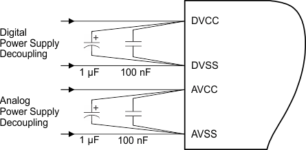 Figure 7-1 Power Supply Decoupling
7.1.2 External Oscillator
Depending on the device variant (see Table 3-1), the device can support a low-frequency crystal (32 kHz) on the LFXT pins, a high-frequency crystal on the HFXT pins, or both. External bypass capacitors for the crystal oscillator pins are required.
It is also possible to apply digital clock signals to the LFXIN and HFXIN input pins that meet the specifications of the respective oscillator if the appropriate LFXTBYPASS or HFXTBYPASS mode is selected. In this case, the associated LFXOUT and HFXOUT pins can be used for other purposes.
Figure 7-2 shows a typical connection diagram.
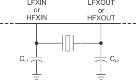 Figure 7-2 Typical Crystal Connection
See the application report MSP430 32-kHz Crystal Oscillators (SLAA322) for more information on selecting, testing, and designing a crystal oscillator with the MSP430 devices.
7.1.3 JTAG
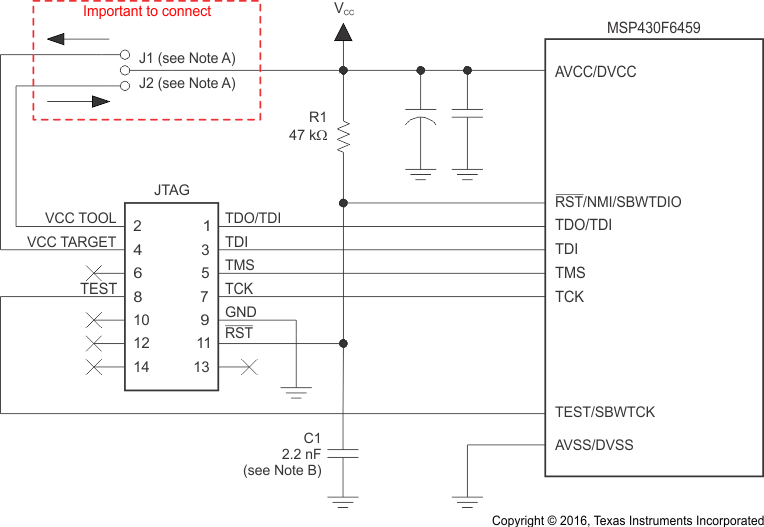
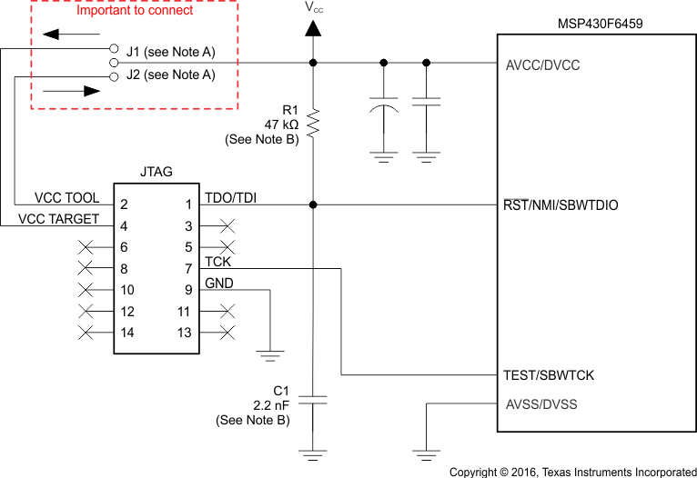
With the proper connections, the debugger and a hardware JTAG interface (such as the MSP-FET or MSP-FET430UIF) can be used to program and debug code on the target board. In addition, the connections also support the MSP-GANG production programmers, thus providing an easy way to program prototype boards, if desired. Figure 7-3 shows the connections between the 14-pin JTAG connector and the target device required to support in-system programming and debugging for 4-wire JTAG communication. Figure 7-4 shows the connections for 2-wire JTAG mode (Spy-Bi-Wire).
The connections for the MSP-FET and MSP-FET430UIF interface modules and the MSP-GANG are identical. Both can supply VCC to the target board (through pin 2). In addition, the MSP-FET and MSP-FET430UIF interface modules and MSP-GANG have a VCC sense feature that, if used, requires an alternate connection (pin 4 instead of pin 2). The VCC-sense feature senses the local VCC present on the target board (that is, a battery or other local power supply) and adjusts the output signals accordingly. Figure 7-3 and Figure 7-4 show a jumper block that supports both scenarios of supplying VCC to the target board. If this flexibility is not required, the desired VCC connections may be hard-wired to eliminate the jumper block. Pins 2 and 4 must not be connected at the same time.
For additional design information regarding the JTAG interface, see the MSP430 Hardware Tools User's Guide (SLAU278).
7.1.4 Reset
The reset pin can be configured as a reset function (default) or as an NMI function in the Special Function Register (SFR), SFRRPCR.
In reset mode, the RST/NMI pin is active low, and a pulse applied to this pin that meets the reset timing specifications generates a BOR-type device reset.
Setting SYSNMI causes the RST/NMI pin to be configured as an external NMI source. The external NMI is edge sensitive, and its edge is selectable by SYSNMIIES. Setting the NMIIE enables the interrupt of the external NMI. When an external NMI event occurs, the NMIIFG is set.
The RST/NMI pin can have either a pullup or pulldown that is enabled or not. SYSRSTUP selects either pullup or pulldown, and SYSRSTRE causes the pullup (default) or pulldown to be enabled (default) or not. If the RST/NMI pin is unused, it is required either to select and enable the internal pullup or to connect an external 47-kΩ pullup resistor to the RST/NMI pin with a 2.2-nF pulldown capacitor. The pulldown capacitor should not exceed 2.2 nF when using devices with Spy-Bi-Wire interface in Spy-Bi-Wire mode or in 4-wire JTAG mode with TI tools like FET interfaces or GANG programmers.
See the MSP430x5xx and MSP430x6xx Family User's Guide (SLAU208) for more information on the referenced control registers and bits.
7.1.5 General Layout Recommendations
- Proper grounding and short traces for external crystal to reduce parasitic capacitance. See the application report MSP430 32-kHz Crystal Oscillators (SLAA322) for recommended layout guidelines.
- Proper bypass capacitors on DVCC, AVCC, and reference pins if used.
- Avoid routing any high-frequency signal close to an analog signal line. For example, keep digital switching signals such as PWM or JTAG signals away from the oscillator circuit.
- Refer to the Circuit Board Layout Techniques design guide (SLOA089) for a detailed discussion of PCB layout considerations. This document is written primarily about op amps, but the guidelines are generally applicable for all mixed-signal applications.
- Proper ESD level protection should be considered to protect the device from unintended high-voltage electrostatic discharge. See the application report MSP430 System-Level ESD Considerations (SLAA530) for guidelines.
7.1.6 Do's and Don'ts
TI recommends powering the AVCC and DVCC pins from the same source. At a minimum, during power up, power down, and device operation, the voltage difference between AVCC and DVCC must not exceed the limits specified in the Absolute Maximum Ratings section. Exceeding the specified limits may cause malfunction of the device including erroneous writes to RAM and FRAM.
7.2 Peripheral- and Interface-Specific Design Information
7.2.1 ADC12_B Peripheral
7.2.1.1 Partial Schematic
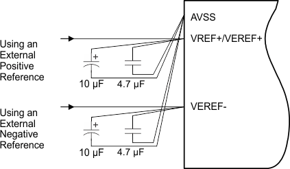 Figure 7-5 ADC12_B Grounding and Noise Considerations
7.2.1.2 Design Requirements
As with any high-resolution ADC, appropriate printed-circuit-board layout and grounding techniques should be followed to eliminate ground loops, unwanted parasitic effects, and noise.
Ground loops are formed when return current from the ADC flows through paths that are common with other analog or digital circuitry. If care is not taken, this current can generate small unwanted offset voltages that can add to or subtract from the reference or input voltages of the ADC. The general guidelines in Section 7.1.1 combined with the connections shown in Section 7.2.1.1 prevent this.
In addition to grounding, ripple and noise spikes on the power-supply lines that are caused by digital switching or switching power supplies can corrupt the conversion result. A noise-free design using separate analog and digital ground planes with a single-point connection is recommend to achieve high accuracy.
Figure 7-5 shows the recommended decoupling circuit when an external voltage reference is used. The internal reference module has a maximum drive current as specified in the Reference module's IO(VREF+) specification.
The reference voltage must be a stable voltage for accurate measurements. The capacitor values that are selected in the general guidelines filter out the high- and low-frequency ripple before the reference voltage enters the device. In this case, the 10-µF capacitor is used to buffer the reference pin and filter any low-frequency ripple. A bypass capacitor of 4.7 µF is used to filter out any high frequency noise.
7.2.1.3 Detailed Design Procedure
For additional design information, see the ADC12_A section in the application report MSP430x5xx and MSP430x6xx Family User's Guide (SLAU208).
7.2.1.4 Layout Guidelines
Component that are shown in the partial schematic (see Figure 7-5) should be placed as close as possible to the respective device pins. Avoid long traces, because they add additional parasitic capacitance, inductance, and resistance on the signal.
Avoid routing analog input signals close to a high-frequency pin (for example, a high-frequency PWM), because the high-frequency switching can be coupled into the analog signal.
If differential mode is used for the ADC12_B, the analog differential input signals must be routed closely together to minimize the effect of noise on the resulting signal.