JAJS271F April 2004 – March 2022 MSP430FG437 , MSP430FG438 , MSP430FG439
PRODUCTION DATA
- 1 特長
- 2 アプリケーション
- 3 概要
- 4 機能ブロック図
- 5 Revision History
- 6 Device Comparison
- 7 Terminal Configuration and Functions
-
8 Specifications
- 8.1 Absolute Maximum Ratings
- 8.2 Handling Ratings
- 8.3 Recommended Operating Conditions
- 8.4 Supply Current Into AVCC + DVCC Excluding External Current
- 8.5 Schmitt-Trigger Inputs – Ports P1 to P6, RST/NMI, JTAG (TCK, TMS, TDI/TCLK, TDO/TDI)
- 8.6 Inputs Px.y, TAx, TBx
- 8.7 Leakage Current – Ports P1 to P6
- 8.8 Outputs – Ports P1 to P6
- 8.9 Output Frequency
- 8.10 Typical Characteristics – Outputs
- 8.11 Wake-Up From LPM3
- 8.12 RAM
- 8.13 LCD
- 8.14 Comparator_A
- 8.15 Comparator_A Typical Characteristics
- 8.16 Power-On Reset (POR) and Brownout Reset (BOR)
- 8.17 Supply Voltage Supervisor (SVS) and Supply Voltage Monitor (SVM)
- 8.18 DCO
- 8.19 Crystal Oscillator, XT1 Oscillator
- 8.20 Crystal Oscillator, XT2 Oscillator
- 8.21 USART0
- 8.22 12-Bit ADC, Power Supply and Input Range Conditions
- 8.23 12-Bit ADC, External Reference
- 8.24 12-Bit ADC, Built-In Reference
- 8.25 12-Bit ADC, Timing Parameters
- 8.26 12-Bit ADC, Linearity Parameters
- 8.27 12-Bit ADC, Temperature Sensor and Built-In VMID
- 8.28 12-Bit DAC, Supply Specifications
- 8.29 12-Bit DAC, Linearity Specifications
- 8.30 12-Bit DAC, Output Specifications
- 8.31 12-Bit DAC, Reference Input Specifications
- 8.32 12-Bit DAC, Dynamic Specifications
- 8.33 12-Bit DAC, Dynamic Specifications (Continued)
- 8.34 Operational Amplifier (OA), Supply Specifications
- 8.35 Operational Amplifier (OA), Input/Output Specifications
- 8.36 Operational Amplifier (OA), Dynamic Specifications
- 8.37 OA Dynamic Specifications Typical Characteristics
- 8.38 Flash Memory
- 8.39 JTAG Interface
- 8.40 JTAG Fuse
-
9 Detailed Description
- 9.1 CPU
- 9.2 Instruction Set
- 9.3 Operating Modes
- 9.4 Interrupt Vector Addresses
- 9.5 Special Function Registers (SFRs)
- 9.6 Memory Organization
- 9.7 Bootstrap Loader (BSL)
- 9.8 Flash Memory
- 9.9
Peripherals
- 9.9.1 DMA Controller
- 9.9.2 Oscillator and System Clock
- 9.9.3 Brownout, Supply Voltage Supervisor
- 9.9.4 Digital I/O
- 9.9.5 Basic Timer1
- 9.9.6 LCD Drive
- 9.9.7 OA
- 9.9.8 Watchdog Timer (WDT)
- 9.9.9 USART0
- 9.9.10 Timer_A3
- 9.9.11 Timer_B3
- 9.9.12 Comparator_A
- 9.9.13 ADC12
- 9.9.14 DAC12
- 9.9.15 Peripheral File Map
- 9.10
Input/Output Schematics
- 9.10.1 Port P1, P1.0 to P1.5, Input/Output With Schmitt Trigger
- 9.10.2 Port P1, P1.6 and P1.7, Input/Output With Schmitt Trigger
- 9.10.3 Port P2, P2.0 and P2.4 to P2.5, Input/Output With Schmitt Trigger
- 9.10.4 Port P2, P2.1 to P2.3, Input/Output With Schmitt Trigger
- 9.10.5 Port P2, P2.6 and P2.7, Input/Output With Schmitt Trigger
- 9.10.6 Port P3, P3.0 to P3.3, Input/Output With Schmitt Trigger
- 9.10.7 Port P3, P3.4 to P3.7, Input/Output With Schmitt Trigger
- 9.10.8 Port P4, P4.0 to P4.5, Input/Output With Schmitt Trigger
- 9.10.9 Port P4, P4.6, Input/Output With Schmitt Trigger
- 9.10.10 Port P4, P4.7, Input/Output With Schmitt Trigger
- 9.10.11 Port P5, P5.0, Input/Output With Schmitt Trigger
- 9.10.12 Port P5, P5.1, Input/Output With Schmitt Trigger
- 9.10.13 Port P5, P5.2 to P5.4, Input/Output With Schmitt Trigger
- 9.10.14 Port P5, P5.5 to P5.7, Input/Output With Schmitt Trigger
- 9.10.15 Port P6, P6.0, P6.2, and P6.4, Input/Output With Schmitt Trigger
- 9.10.16 Port P6, P6.1, Input/Output With Schmitt Trigger
- 9.10.17 Port P6, P6.3, Input/Output With Schmitt Trigger
- 9.10.18 Port P6, P6.5, Input/Output With Schmitt Trigger
- 9.10.19 Port P6, P6.6, Input/Output With Schmitt Trigger
- 9.10.20 Port P6, P6.7, Input/Output With Schmitt Trigger
- 9.10.21 VeREF+/DAC0
- 9.10.22 JTAG Pins TMS, TCK, TDI/TCLK, TDO/TDI, Input/Output With Schmitt Trigger or Output
- 9.10.23 JTAG Fuse Check Mode
- 10Device and Documentation Support
- 11Mechanical Packaging and Orderable Information
パッケージ・オプション
メカニカル・データ(パッケージ|ピン)
サーマルパッド・メカニカル・データ
発注情報
8.3 Recommended Operating Conditions
| MIN | NOM | MAX | UNIT | |||||
|---|---|---|---|---|---|---|---|---|
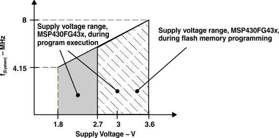
| VCC | Supply voltage(1) (AVCC = DVCC1 = DVCC2 = VCC) | During program execution | 1.8 | 3.6 | V | |||
| During program execution, SVS enabled and PORON = 1(2) | 2 | 3.6 | ||||||
| During flash memory programming | 2.7 | 3.6 | ||||||
| VSS | Supply voltage(1) (AVSS = DVSS1 = DVSS2 = VSS) | 0 | 0 | V | ||||
| TA | Operating free-air temperature range | –40 | 85 | °C | ||||
| f(LFXT1) | XT1 crystal frequency(3) | LF selected, XTS_FLL = 0 | Watch crystal | 32.768 | kHz | |||
| XT1 selected, XTS_FLL = 1 | Ceramic resonator | 450 | 8000 | |||||
| XT1 selected, XTS_FLL = 1 | Crystal | 1000 | 8000 | |||||
| f(XT2) | XT2 crystal frequency | Ceramic resonator | 450 | 8000 | kHz | |||
| Crystal | 1000 | 8000 | ||||||
| f(System) | Processor frequency (signal MCLK) | VCC = 1.8 V | dc | 4.15 | MHz | |||
| VCC = 3.6 V | dc | 8 | ||||||
(1) It is recommended to power AVCC and DVCC from the same source. A maximum difference of 0.3 V between AVCC and DVCC can be tolerated during power up and operation.
(2) The minimum operating supply voltage is defined according to the trip point where POR is going active by decreasing the supply voltage. POR is going inactive when the supply voltage is raised above the minimum supply voltage plus the hysteresis of the SVS circuitry.
(3) In LF mode, the LFXT1 oscillator requires a watch crystal. In XT1 mode, LFXT1 accepts a ceramic resonator or a crystal.
 Figure 8-1 Frequency vs Supply Voltage, Typical Characteristic