JAJSCD6E August 2016 – June 2021 MSP430FR2000 , MSP430FR2100 , MSP430FR2110 , MSP430FR2111
PRODUCTION DATA
- 1 特長
- 2 アプリケーション
- 3 概要
- 4 機能ブロック図
- 5 Revision History
- 6 Device Comparison
- 7 Terminal Configuration and Functions
-
8 Specifications
- 8.1 Absolute Maximum Ratings
- 8.2 ESD Ratings
- 8.3 Recommended Operating Conditions
- 8.4 Active Mode Supply Current Into VCC Excluding External Current
- 8.5 Active Mode Supply Current Per MHz
- 8.6 Low-Power Mode LPM0 Supply Currents Into VCC Excluding External Current
- 8.7 Low-Power Mode LPM3, LPM4 Supply Currents (Into VCC) Excluding External Current
- 8.8 Low-Power Mode LPMx.5 Supply Currents (Into VCC) Excluding External Current
- 8.9 Typical Characteristics – LPM Supply Currents
- 8.10 Current Consumption Per Module
- 8.11 Thermal Resistance Characteristics
- 8.12 Timing and Switching Characteristics
-
9 Detailed Description
- 9.1 Overview
- 9.2 CPU
- 9.3 Operating Modes
- 9.4 Interrupt Vector Addresses
- 9.5 Memory Organization
- 9.6 Bootloader (BSL)
- 9.7 JTAG Standard Interface
- 9.8 Spy-Bi-Wire Interface (SBW)
- 9.9 FRAM
- 9.10 Memory Protection
- 9.11
Peripherals
- 9.11.1 Power-Management Module (PMM) and On-Chip Reference Voltages
- 9.11.2 Clock System (CS) and Clock Distribution
- 9.11.3 General-Purpose Input/Output Port (I/O)
- 9.11.4 Watchdog Timer (WDT)
- 9.11.5 System Module (SYS)
- 9.11.6 Cyclic Redundancy Check (CRC)
- 9.11.7 Enhanced Universal Serial Communication Interface (eUSCI_A0)
- 9.11.8 Timers (Timer0_B3)
- 9.11.9 Backup Memory (BAKMEM)
- 9.11.10 Real-Time Clock (RTC) Counter
- 9.11.11 10-Bit Analog-to-Digital Converter (ADC)
- 9.11.12 eCOMP0
- 9.11.13 Embedded Emulation Module (EEM)
- 9.11.14 Peripheral File Map
- 9.11.15 Input/Output Diagrams
- 9.12 Device Descriptors (TLV)
- 9.13 Identification
- 10Applications, Implementation, and Layout
- 11Device and Documentation Support
- 12Mechanical, Packaging, and Orderable Information
パッケージ・オプション
メカニカル・データ(パッケージ|ピン)
サーマルパッド・メカニカル・データ
- RLL|24
発注情報
11.2 Device Nomenclature
To designate the stages in the product development cycle, TI assigns prefixes to the part numbers of all MSP MCU devices. Each MSP MCU commercial family member has one of two prefixes: MSP or XMS. These prefixes represent evolutionary stages of product development from engineering prototypes (XMS) through fully qualified production devices (MSP).
XMS – Experimental device that is not necessarily representative of the final device's electrical specifications
MSP – Fully qualified production device
XMS devices are shipped against the following disclaimer:
"Developmental product is intended for internal evaluation purposes."
MSP devices have been characterized fully, and the quality and reliability of the device have been demonstrated fully. TI's standard warranty applies.
Predictions show that prototype devices (XMS) have a greater failure rate than the standard production devices. TI recommends that these devices not be used in any production system because their expected end-use failure rate still is undefined. Only qualified production devices are to be used.
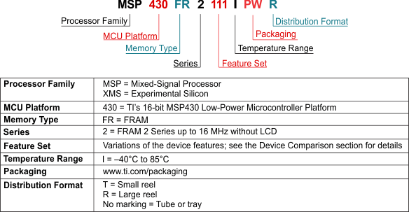
TI device nomenclature also includes a suffix with the device family name. This suffix indicates the temperature range, package type, and distribution format. #SLASE788152 provides a legend for reading the complete device name.
 Figure 11-1 Device Nomenclature