JAJSCZ4E January 2017 – December 2022 OPA1677 , OPA1678 , OPA1679
PRODUCTION DATA
- 1 特長
- 2 アプリケーション
- 3 概要
- 4 Revision History
- 5 Pin Configuration and Functions
- 6 Specifications
- 7 Detailed Description
-
8 Application and Implementation
- 8.1 Application Information
- 8.2 Typical Applications
- 8.3 Power Supply Recommendations
- 8.4 Layout
- 9 Device and Documentation Support
- 10Mechanical, Packaging, and Orderable Information
パッケージ・オプション
メカニカル・データ(パッケージ|ピン)
サーマルパッド・メカニカル・データ
- RUM|16
発注情報
5 Pin Configuration and Functions
Figure 5-1 OPA1677: D Package, 8-Pin
SOIC (Top View)
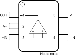
 Figure 5-2 OPA1677: DBV Package,
5-Pin SOT-23 (Top View)
Figure 5-2 OPA1677: DBV Package,
5-Pin SOT-23 (Top View)Pin Functions: OPA1677
| PIN | TYPE | DESCRIPTION | ||
|---|---|---|---|---|
| NAME | NO. | |||
| D (SOIC) |
DBV (SOT-23) | |||
| –IN | 2 | 4 | Input | Inverting input |
| +IN | 3 | 3 | Input | Noninverting input |
| OUT | 6 | 1 | Output | Output |
| V– | 4 | 2 | Power | Negative (lowest) power supply |
| V+ | 7 | 5 | Power | Positive (highest) power supply |
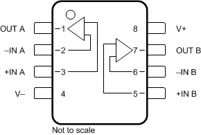
 Figure 5-3 OPA1678: D Package, 8-Pin
SOIC and DGK Package, 8-Pin VSSOP (Top View)
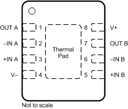
 Figure 5-4 OPA1678: DRG Package,
8-Pin SON With Exposed Thermal Pad (Top View)
Figure 5-4 OPA1678: DRG Package,
8-Pin SON With Exposed Thermal Pad (Top View)Pin Functions:
OPA1678
| PIN | TYPE | DESCRIPTION | |
|---|---|---|---|
| NAME | NO. | ||
| –IN A | 2 | Input | Inverting input, channel A |
| +IN A | 3 | Input | Noninverting input, channel A |
| –IN B | 6 | Input | Inverting input, channel B |
| +IN B | 5 | Input | Noninverting input, channel B |
| OUT A | 1 | Output | Output, channel A |
| OUT B | 7 | Output | Output, channel B |
| V– | 4 | Power | Negative (lowest) power supply |
| V+ | 8 | Power | Positive (highest) power supply |
| Thermal Pad | Thermal pad | — | For DRG (SON-8) package. Exposed thermal die pad on underside. Connect thermal die pad to V–. Solder the thermal pad to improve heat dissipation and provide specified performance. |
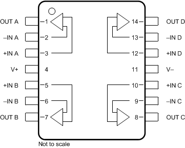
 Figure 5-5 OPA1679: D Package,
14-Pin SOIC and
 PW Package, 14-Pin TSSOP (Top View)
Figure 5-6 OPA1679: RUM Package,
16-Pin QFN With Exposed Thermal Pad (Top View)
Pin Functions:
OPA1679
| PIN | TYPE | DESCRIPTION | ||
|---|---|---|---|---|
| NAME | NO. | |||
| D (SOIC) PW (TSSOP) |
RUM (QFN) | |||
| –IN A | 2 | 1 | Input | Inverting input, channel A |
| +IN A | 3 | 2 | Input | Noninverting input, channel A |
| –IN B | 6 | 5 | Input | Inverting input, channel B |
| +IN B | 5 | 4 | Input | Noninverting input, channel B |
| –IN C | 9 | 8 | Input | Inverting input, channel C |
| +IN C | 10 | 9 | Input | Noninverting input, channel C |
| –IN D | 13 | 12 | Input | Inverting input, channel D |
| +IN D | 12 | 11 | Input | Noninverting input, channel D |
| NC | — | 13 | — | No connect |
| NC | — | 16 | — | No connect |
| OUT A | 1 | 15 | Output | Output, channel A |
| OUT B | 7 | 6 | Output | Output, channel B |
| OUT C | 8 | 7 | Output | Output, channel C |
| OUT D | 14 | 14 | Output | Output, channel D |
| V+ | 4 | 3 | Power | Positive (highest) power supply |
| V– | 11 | 10 | Power | Negative (lowest) power supply |
| Thermal Pad | — | Thermal pad | — | Exposed thermal die pad on underside. Connect thermal die pad to V–. Solder the thermal pad to improve heat dissipation and provide specified performance. |