JAJSDY5E October   2017  – February 2020 OPA202 , OPA2202 , OPA4202

PRODUCTION DATA.  

  1. 特長
  2. アプリケーション
  3. 概要
    1.     OPAx202 は大きな容量性負荷を直接駆動しても優れた性能を発揮
  4. 改訂履歴
  5. Pin Configuration and Functions
    1.     Pin Functions: OPA202
    2.     Pin Functions: OPA2202
    3.     Pin Functions: OPA4202
  6. Specifications
    1. 6.1 Absolute Maximum Ratings
    2. 6.2 ESD Ratings
    3. 6.3 Recommended Operating Conditions
    4. 6.4 Thermal Information: OPA202
    5. 6.5 Thermal Information: OPA2202
    6. 6.6 Thermal Information: OPA4202
    7. 6.7 Electrical Characteristics
    8. 6.8 Typical Characteristics
    9. 6.9 Typical Characteristics
  7. Detailed Description
    1. 7.1 Overview
    2. 7.2 Functional Block Diagram
    3. 7.3 Feature Description
      1. 7.3.1 Capacitive Load and Stability
      2. 7.3.2 Output Current Limit
      3. 7.3.3 Noise Performance
      4. 7.3.4 Phase-Reversal Protection
      5. 7.3.5 Thermal Protection
      6. 7.3.6 Electrical Overstress
      7. 7.3.7 EMI Rejection
      8. 7.3.8 EMIRR +IN Test Configuration
    4. 7.4 Device Functional Modes
  8. Application and Implementation
    1. 8.1 Application Information
      1. 8.1.1 Basic Noise Calculations
    2. 8.2 Typical Application
      1. 8.2.1 Design Requirements
      2. 8.2.2 Detailed Design Procedure
      3. 8.2.3 Application Curve
  9. Power Supply Recommendations
  10. 10Layout
    1. 10.1 Layout Guidelines
    2. 10.2 Layout Example
  11. 11デバイスおよびドキュメントのサポート
    1. 11.1 デバイス・サポート
      1. 11.1.1 開発サポート
        1. 11.1.1.1 TINA-TI(無料のダウンロード・ソフトウェア)
        2. 11.1.1.2 WEBENCH Filter Designerツール
        3. 11.1.1.3 TI Precision Designs
    2. 11.2 ドキュメントのサポート
      1. 11.2.1 関連資料
    3. 11.3 関連リンク
    4. 11.4 ドキュメントの更新通知を受け取る方法
    5. 11.5 サポート・リソース
    6. 11.6 商標
    7. 11.7 静電気放電に関する注意事項
    8. 11.8 Glossary
  12. 12メカニカル、パッケージ、および注文情報

パッケージ・オプション

メカニカル・データ(パッケージ|ピン)
サーマルパッド・メカニカル・データ
発注情報

Basic Noise Calculations

Low-noise circuit design requires careful analysis of all noise sources. External noise sources dominates in many cases; consider the effect of source resistance on overall op amp noise performance. Total noise of the circuit is the root-sum-square combination of all noise components.

The resistive portion of the source impedance produces thermal noise proportional to the square root of the resistance. Figure 42 shows this function. The source impedance is usually fixed; consequently, select the op amp and the feedback resistors to minimize the respective contributions to the total noise.

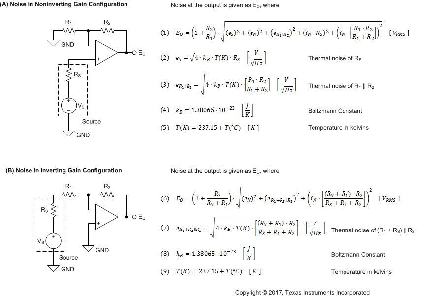
Figure 46 shows noninverting (A) and inverting (B) op amp circuit configurations with gain. In circuit configurations with gain, the feedback network resistors contribute noise. Typically, the current noise of the op amp reacts with the feedback resistors to create additional noise components. However, the extremely low current noise of the OPAx202 means that the current noise contribution is neglected.

The feedback resistor values are typically selected to make these noise sources negligible. Low impedance feedback resistors load the output of the amplifier. The equations for total noise are shown for both configurations.
OPA202 OPA2202 OPA4202 S008_SBOS427.gif
eN = the voltage noise of the amplifier = 9 nV/√Hz at 1 kHz.
iN = the current noise of the amplifier = 76 fA/√Hz at 1 kHz.
For additional resources on noise calculations, visit TI's Precision Labs.
Figure 46. Noise Calculation in Gain Configurations