JAJSG31B September   2018  – June 2019 OPA2156

PRODUCTION DATA.  

  1. 特長
  2. アプリケーション
  3. 概要
    1.     Device Images
      1.      入力電圧のノイズ・スペクトル密度が低い
      2.      OPA2156 トランスインピーダンス構成
  4. 改訂履歴
  5. 概要(続き)
  6. Pin Configuration and Functions
    1.     Pin Functions
  7. Specifications
    1. 7.1 Absolute Maximum Ratings
    2. 7.2 ESD Ratings
    3. 7.3 Recommended Operating Conditions
    4. 7.4 Thermal Information: OPA2156
    5. 7.5 Electrical Characteristics
    6. 7.6 Typical Characteristics
  8. Detailed Description
    1. 8.1 Overview
    2. 8.2 Functional Block Diagram
    3. 8.3 Feature Description
      1. 8.3.1 Phase Reversal Protection
      2. 8.3.2 Electrical Overstress
      3. 8.3.3 Thermal Considerations
      4. 8.3.4 Thermal Shutdown
      5. 8.3.5 Common-Mode Voltage Range
      6. 8.3.6 Overload Recovery
    4. 8.4 Device Functional Modes
  9. Application and Implementation
    1. 9.1 Application Information
      1. 9.1.1 Slew Rate Limit for Input Protection
    2. 9.2 Typical Application
      1. 9.2.1 Design Requirements
      2. 9.2.2 Detailed Design Procedure
      3. 9.2.3 Application Curves
  10. 10Power Supply Recommendations
  11. 11Layout
    1. 11.1 Layout Guidelines
      1. 11.1.1 Power Dissipation
    2. 11.2 Layout Example
  12. 12デバイスおよびドキュメントのサポート
    1. 12.1 デバイス・サポート
      1. 12.1.1 開発サポート
        1. 12.1.1.1 TINA-TI(無料のダウンロード・ソフトウェア)
        2. 12.1.1.2 TI Precision Designs
    2. 12.2 ドキュメントのサポート
      1. 12.2.1 関連資料
    3. 12.3 ドキュメントの更新通知を受け取る方法
    4. 12.4 コミュニティ・リソース
    5. 12.5 商標
    6. 12.6 静電気放電に関する注意事項
    7. 12.7 Glossary
  13. 13メカニカル、パッケージ、および注文情報

パッケージ・オプション

メカニカル・データ(パッケージ|ピン)
サーマルパッド・メカニカル・データ
発注情報

Detailed Design Procedure

In this example the OPA2156 serves as a transimpedance amplifier for a differential photodiode. The differential configuration allows for a wider output range (0 to 10-V differential) compared to a single-ended configuration (0 V to 5 V). This output can be connected to a differential successive approximation register (SAR) analog-to-digital converter (ADC). The basic equation for a differential transimpedance amplifier output voltage is shown in Equation 3.

Equation 3. OPA2156 Eq3-Transimpedance.gif

Equation 3 can be rearranged to calculate the value of the feedback resistors as shown in Equation 4.
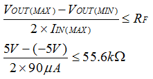
Equation 4. OPA2156 Eq4-Feedback_Resistor.gif

Adding a capacitor to the feedback loop creates a filter which will remove undesired noise beyond its cutoff frequency. For this application a 1-MHz cutoff frequency was selected. The equation for an RC filter is provided in Equation 5.

Equation 5. OPA2156 Eq5-Cutoff_Frequency.gif

Rearranging this equation to solve for the capacitor value is show in Equation 6.

Equation 6. OPA2156 Eq6-Feedback_Capacitor.gif

For more information on photodiode transimpedance amplifier system design and for a single-ended example, see TIDU535: 1 MHz, Single-Supply, Photodiode Amplifier Reference Design.