JAJSFF7F June   2009  – May 2018 OPA2354A-Q1 , OPA354A-Q1 , OPA4354-Q1

PRODUCTION DATA.  

  1. 特長
  2. アプリケーション
  3. 概要
    1.     概略回路図
  4. 改訂履歴
  5. Pin Configuration and Functions
    1.     Pin Functions: OPA354A-Q1
    2.     Pin Functions: OPA2354A-Q1
    3.     Pin Functions: OPA4354-Q1
  6. Specifications
    1. 6.1 Absolute Maximum Ratings
    2. 6.2 ESD Ratings
    3. 6.3 Recommended Operating Conditions
    4. 6.4 Thermal Information: OPA354A-Q1
    5. 6.5 Thermal Information: OPA2354A-Q1
    6. 6.6 Thermal Information: OPA4354A-Q1
    7. 6.7 Electrical Characteristics
    8. 6.8 Typical Characteristics
  7. Detailed Description
    1. 7.1 Overview
    2. 7.2 Functional Block Diagram
    3. 7.3 Feature Description
      1. 7.3.1 Operating Voltage
      2. 7.3.2 Rail-to-Rail Input
      3. 7.3.3 Rail-to-Rail Output
      4. 7.3.4 Output Drive
      5. 7.3.5 Video
      6. 7.3.6 Driving Analog-to-Digital Converters
      7. 7.3.7 Capacitive Load and Stability
      8. 7.3.8 Wideband Transimpedance Amplifier
    4. 7.4 Device Functional Modes
  8. Application and Implementation
    1. 8.1 Application Information
    2. 8.2 Typical Applications
      1. 8.2.1 Transimpedance Amplifier
        1. 8.2.1.1 Design Requirements
        2. 8.2.1.2 Detailed Design Procedure
          1. 8.2.1.2.1 Optimizing The Transimpedance Circuit
        3. 8.2.1.3 Application Curve
      2. 8.2.2 High-Impedance Sensor Interface
      3. 8.2.3 Driving ADCs
      4. 8.2.4 Active Filter
  9. Power Supply Recommendations
    1. 9.1 Power Dissipation
  10. 10Layout
    1. 10.1 Layout Guidelines
    2. 10.2 Layout Example
  11. 11デバイスおよびドキュメントのサポート
    1. 11.1 ドキュメントのサポート
      1. 11.1.1 関連資料
    2. 11.2 関連リンク
    3. 11.3 ドキュメントの更新通知を受け取る方法
    4. 11.4 コミュニティ・リソース
    5. 11.5 商標
    6. 11.6 静電気放電に関する注意事項
    7. 11.7 Glossary
  12. 12メカニカル、パッケージ、および注文情報

パッケージ・オプション

メカニカル・データ(パッケージ|ピン)
サーマルパッド・メカニカル・データ
発注情報

Driving Analog-to-Digital Converters

The OPAx354-Q1 family of op-amps offers a 60-ns settling time to 0.01%, which makes the devices a viable option for driving high- and medium-speed sampling ADCs and reference circuits. The OPAx354-Q1 family of devices provides an effective means of buffering the input capacitance and resulting charge injection of the ADC while providing signal gain. The OPAx354-Q1 family of devices is designed for applications requiring high DC accuracy.

Figure 34 shows the OPAx354-Q1 family of devices driving an ADC. With the OPAx354-Q1 family of devices in an inverting configuration, using a capacitor across the feedback resistor can filter high-frequency noise in the signal.
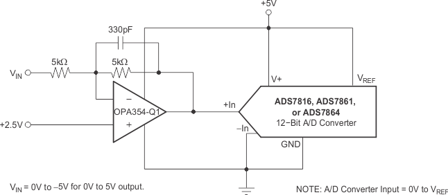
OPA354A-Q1 OPA2354A-Q1 OPA4354-Q1 ai_invert_confg_ads_bos492.gifFigure 34. OPA354A-Q1 Inverting Configuration Driving the ADS7816