JAJSFF7F June   2009  – May 2018 OPA2354A-Q1 , OPA354A-Q1 , OPA4354-Q1

PRODUCTION DATA.  

  1. 特長
  2. アプリケーション
  3. 概要
    1.     概略回路図
  4. 改訂履歴
  5. Pin Configuration and Functions
    1.     Pin Functions: OPA354A-Q1
    2.     Pin Functions: OPA2354A-Q1
    3.     Pin Functions: OPA4354-Q1
  6. Specifications
    1. 6.1 Absolute Maximum Ratings
    2. 6.2 ESD Ratings
    3. 6.3 Recommended Operating Conditions
    4. 6.4 Thermal Information: OPA354A-Q1
    5. 6.5 Thermal Information: OPA2354A-Q1
    6. 6.6 Thermal Information: OPA4354A-Q1
    7. 6.7 Electrical Characteristics
    8. 6.8 Typical Characteristics
  7. Detailed Description
    1. 7.1 Overview
    2. 7.2 Functional Block Diagram
    3. 7.3 Feature Description
      1. 7.3.1 Operating Voltage
      2. 7.3.2 Rail-to-Rail Input
      3. 7.3.3 Rail-to-Rail Output
      4. 7.3.4 Output Drive
      5. 7.3.5 Video
      6. 7.3.6 Driving Analog-to-Digital Converters
      7. 7.3.7 Capacitive Load and Stability
      8. 7.3.8 Wideband Transimpedance Amplifier
    4. 7.4 Device Functional Modes
  8. Application and Implementation
    1. 8.1 Application Information
    2. 8.2 Typical Applications
      1. 8.2.1 Transimpedance Amplifier
        1. 8.2.1.1 Design Requirements
        2. 8.2.1.2 Detailed Design Procedure
          1. 8.2.1.2.1 Optimizing The Transimpedance Circuit
        3. 8.2.1.3 Application Curve
      2. 8.2.2 High-Impedance Sensor Interface
      3. 8.2.3 Driving ADCs
      4. 8.2.4 Active Filter
  9. Power Supply Recommendations
    1. 9.1 Power Dissipation
  10. 10Layout
    1. 10.1 Layout Guidelines
    2. 10.2 Layout Example
  11. 11デバイスおよびドキュメントのサポート
    1. 11.1 ドキュメントのサポート
      1. 11.1.1 関連資料
    2. 11.2 関連リンク
    3. 11.3 ドキュメントの更新通知を受け取る方法
    4. 11.4 コミュニティ・リソース
    5. 11.5 商標
    6. 11.6 静電気放電に関する注意事項
    7. 11.7 Glossary
  12. 12メカニカル、パッケージ、および注文情報

パッケージ・オプション

メカニカル・データ(パッケージ|ピン)
サーマルパッド・メカニカル・データ
発注情報

Wideband Transimpedance Amplifier

Wide bandwidth, low-input bias current, and low input voltage and current noise make the OPAx354-Q1 family of devices is designed as a wideband photodiode transimpedance amplifier for low-voltage single-supply applications. Low-voltage noise is important because photodiode capacitance causes the effective noise gain of the circuit to increase at high frequency.

The key elements to a transimpedance design, as shown in Figure 36, are the expected diode capacitance [including the parasitic input common-mode and differential-mode input capacitance (2 + 2) pF for the OPAx354-Q1], the desired transimpedance gain (RF), and the gain-bandwidth product (GBW) for the OPAx354-Q1 family of devices (100 MHz). With these three variables set, the feedback capacitor value (CF) is set to control the frequency response.
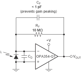
OPA354A-Q1 OPA2354A-Q1 OPA4354-Q1 ai_transimped_amp_bos492.gifFigure 36. Transimpedance Amplifier

To achieve a maximally flat second-order Butterworth frequency response, set the feedback pole as shown in Equation 1.

Equation 1. OPA354A-Q1 OPA2354A-Q1 OPA4354-Q1 ai_eq_1_bos492.gif

Typical surface-mount resistors have a parasitic capacitance of approximately 0.2 pF that required deduction from the calculated feedback capacitance value.

Use Equation 2 to calculate the bandwidth.

Equation 2. OPA354A-Q1 OPA2354A-Q1 OPA4354-Q1 ai_eq_2_bos492.gif

For even higher transimpedance bandwidth, use the high-speed CMOS OPA355-Q1 (200-MHz GBW) or the OPA655-Q1 (400-MHz GBW).