SBOS940A May 2019 – March 2020 OPA818
PRODUCTION DATA.
- 1 Features
- 2 Applications
- 3 Description
- 4 Revision History
- 5 Device Comparison Table
- 6 Pin Configuration and Functions
- 7 Specifications
- 8 Detailed Description
- 9 Application and Implementation
- 10Power Supply Recommendations
- 11Layout
- 12Device and Documentation Support
- 13Mechanical, Packaging, and Orderable Information
パッケージ・オプション
メカニカル・データ(パッケージ|ピン)
- DRG|8
サーマルパッド・メカニカル・データ
- DRG|8
発注情報
9.2.1.2 Detailed Design Procedure
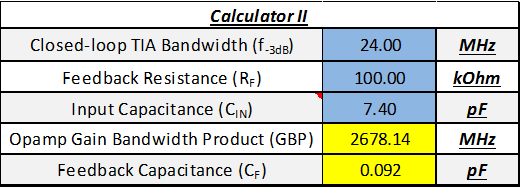
Designs that require high bandwidth from a large area detector with relatively high transimpedance gain benefit from the low input voltage noise of the OPA818. This input voltage noise is peaked up over frequency by the diode source capacitance, and can, in many cases, become the limiting factor to input sensitivity. Figure 51 shows the transimpedance circuit with the parameters as defined in Design Requirements. To use the Microsoft Excel™ calculator available at What You Need To Know About Transimpedance Amplifiers – Part 1 to help with the component selection, total input capacitance, CTOT, needs to be determined. CTOT is referred as CIN in the calculator. CTOT is the sum of CD, CDIFF, and CCM which is 7.4 pF. Using this value of CTOT, and the targeted closed-loop bandwidth (f–3dB) of 24 MHz and transimpedance gain of 100 kΩ results in a need for an amplifier with approximately 2.68 GHz GBWP and a feedback capacitance (CF) of 0.092 pF as shown in Figure 52. These results are for a Butterworth response with a Q = 0.707 and a phase margin of approximately 65° which corresponds to 4.3% overshoot.
 Figure 52. Results of Inputting Design Parameters in the TIA Calculator
 With OPA818's 2.7 GHz GBWP, it will be a suitable amplifier for the design requirements. A challenge with the calculated component results is practically realizing a 0.092 pF capacitor. Such a small capacitor can be realized by using a capacitive tee network formed by C1, C2, and CT such as that shown in Figure 51. The equivalent capacitance, CEQ, of the tee network is given by .
The tee network forms a capacitive attenuator from input to output with C1 and CT, and from output to input with C2 and CT. With the value of CT being higher than C1 or C2, only a fraction of the output signal is seen by C1. This results in a much smaller shunting current provided to the input through C1 and this reduced shunting current effect is equivalent to how a much smaller capacitor behaves (at a fixed frequency, smaller capacitor has higher impedance and thus reduced current). It is recommended to keep the same level of attenuation from input to output and vice versa. To find the appropriate capacitor values for the tee network, chose an arbitrarily low but practically realizable and equal values for capacitors C1 and C2, set CEQ = CTOT, and use to get the value of the tunable capacitor, CT. The values of capacitors C1, C2, and CT in Figure 51 were determined using this process.
Figure 53 shows the TINA simulated closed-loop bandwidth response of the circuit in Figure 51. The circuit was designed for f–3dB = 24 MHz and the simulated closed-loop 3-dB frequency is 24.6 MHz with about 0.1 dB peaking. The OPA818 TINA model models the input common-mode and differential capacitors so they should not be added externally when simulating in TINA. The noise simulation of the TIA circuit is shown in Figure 54. The output referred voltage noise is shown on the Y-axis to the left and the input referred current noise, which is essentially output referred voltage noise divided by the transimpedance gain of 100k, is shown on the secondary Y-axis to the right. The simulation results are fairly accurate because the OPA818 TINA model closely models the voltage and current noise performance of the amplifier. The flat-band output voltage noise is 41 nV/√Hz that is equivalent to 0.41 pA/√Hz of input referred current noise. The noise in relatively low frequency region where the noise gain of the amplifier is 1 V/V is dominated by the thermal noise of the 100 kΩ resistor (40.7 nV/√Hz at 27°C). At mid frequencies beyond the zero formed by RF and CTOT, the noise gain of the amplifier amplifies the voltage noise of the amplifier. The amplifier's noise starts to become the dominant noise contributor from this frequency onwards before the output noise starts to roll off at frequencies beyond the 3-dB closed-loop bandwidth. When looked at integrated root-mean-square (RMS) noise, the mid-frequency noise will be a significant contributor and hence using a 2.2 nV/√Hz low-noise amplifier like OPA818 is advantageous to minimize total RMS noise in the system.