SBOS940A May 2019 – March 2020 OPA818
PRODUCTION DATA.
- 1 Features
- 2 Applications
- 3 Description
- 4 Revision History
- 5 Device Comparison Table
- 6 Pin Configuration and Functions
- 7 Specifications
- 8 Detailed Description
- 9 Application and Implementation
- 10Power Supply Recommendations
- 11Layout
- 12Device and Documentation Support
- 13Mechanical, Packaging, and Orderable Information
パッケージ・オプション
メカニカル・データ(パッケージ|ピン)
- DRG|8
サーマルパッド・メカニカル・データ
- DRG|8
発注情報
9.1.2 Wideband, Transimpedance Design Using OPA818
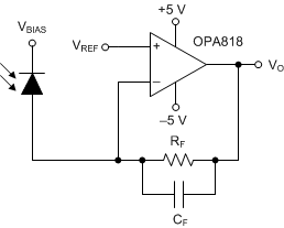
With high GBWP, low input voltage and current noise, and low input capacitance, the OPA818 design is optimized for wideband, low-noise transimpedance applications. The high voltage capability allows greater flexibility of supply voltages along with wider output voltage swings. Figure 50 shows an example circuit of a typical photodiode amplifier circuit. Generally the photodiode is reverse biased in a TIA application so the photodiode current in the circuit of Figure 50 flows into the op amp feedback loop resulting in an output voltage that reduces from VREF with increasing photodiode current. In this type of configuration and depending on the application needs, VREF can be biased closer to VS+ to achieve the desired output swing. Input common-mode range must be considered so as not to violate it when VREF bias is used.
The key design elements that determine the closed-loop bandwidth, f–3dB, of the circuit are below:
- The op amp GBWP.
- The transimpedance gain, RF.
- The total input capacitance, CTOT, that includes photodiode capacitance, input capacitance of the amplifier (common-mode and differential capacitance), and PCB parasitic capacitance.
 Figure 50. Wideband, Low-Noise, Transimpedance Amplifier
 shows the relationship between the above mentioned three elements for a Butterworth response.
The feedback resistance, RF and the total input capacitance, CTOT cause a zero in the noise gain that results in instability if left uncompensated. To counteract the effect of the zero, a pole is inserted in the noise gain by adding the feedback capacitor, CF. The Transimpedance Considerations for High-Speed Amplifiers application report discusses theories and equations that show how to compensate a transimpedance amplifier for a particular gain and input capacitance. The bandwidth and compensation equations from the application report are available in a Microsoft Excel™ calculator. What You Need To Know About Transimpedance Amplifiers – Part 1 provides a link to the calculator. The details of maximizing the dynamic range of TIA front-ends as shown in High-Speed Optical Front-End that uses voltages VREF1 and VREF2 are provided in Maximizing the dynamic range of analog TIA front-end application note.