SCPS144C May 2006 – May 2015 P82B96
PRODUCTION DATA.
- 1 Features
- 2 Applications
- 3 Description
- 4 Revision History
- 5 Description (continued)
- 6 Pin Configuration and Functions
-
7 Specifications
- 7.1 Absolute Maximum Ratings
- 7.2 ESD Ratings
- 7.3 Recommended Operating Conditions
- 7.4 Thermal Information
- 7.5 Electrical Characteristics: VCC = 2.3 V to 2.7 V
- 7.6 Electrical Characteristics: VCC = 3 V to 3.6 V
- 7.7 Electrical Characteristics: VCC = 4.5 V to 5.5 V
- 7.8 Electrical Characteristics: VCC = 15 V
- 7.9 Switching Characteristics
- 7.10 Typical Characteristics
- 8 Parameter Measurement Information
- 9 Detailed Description
- 10Application and Implementation
- 11Power Supply Recommendations
- 12Layout
- 13Device and Documentation Support
- 14Mechanical, Packaging, and Orderable Information
パッケージ・オプション
メカニカル・データ(パッケージ|ピン)
サーマルパッド・メカニカル・データ
発注情報
10 Application and Implementation
NOTE
Information in the following applications sections is not part of the TI component specification, and TI does not warrant its accuracy or completeness. TI’s customers are responsible for determining suitability of components for their purposes. Customers should validate and test their design implementation to confirm system functionality.
10.1 Application Information
10.1.1 Calculating System Delays and Bus-Clock Frequency for Fast Mode System
Figure 7 through Figure 9 show the P82B96 used to drive extended bus wiring, with relatively large capacitance (up to 4000 pF), linking two Fast mode I2C bus nodes. It includes simplified expressions for making the relevant timing calculations for 3.3-/5-V operation. It may be necessary to decrease the nominal SCL frequency below 400 kHz, because the buffers and the wiring introduce timing delays. In most cases, the actual bus frequency is lower than the nominal master timing, due to bit-wise stretching of the clock periods.
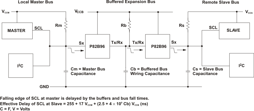 Figure 7. Linking Two I2C Bus Nodes Over a Long Cable, Master to Slave
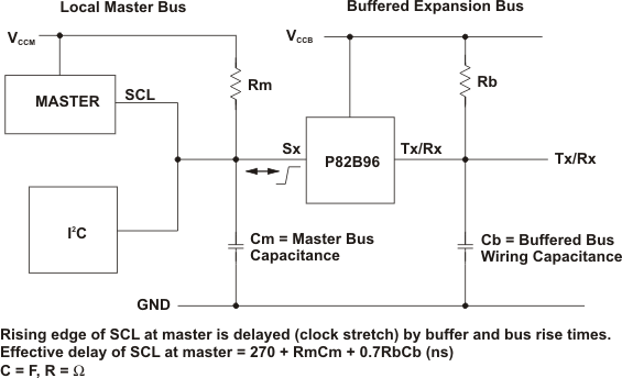 Figure 8. Master I2C Node Connection to P82B96
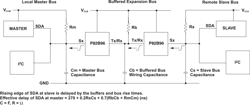 Figure 9. Linking Two I2C Bus Nodes Over a Long Cable, Slave to Master
The delay factors involved in calculation of the allowed bus speed are:
- The propagation delay of the master signal through the buffers and wiring to the slave. The important delay is that of the falling edge of SCL, because this edge requests the data or ACK from a slave.
- The effective stretching of the nominal low period of SCL at the master, caused by the buffer and bus rise times.
- The propagation delay of the slave response signal through the buffers and wiring back to the master. The important delay is that of a rising edge in the SDA signal. Rising edges always are slower and, therefore, are delayed by a longer time than falling edges. (The rising edges are limited by the passive pullup, while falling edges actively are driven.)
The timing requirement in any I2C system is that a slave’s data response (which is provided in response to a falling edge of SCL) must be received at the master before the end of the corresponding low period of SCL as it appears on the bus wiring at the master. Because all slaves, as a minimum, satisfy the worst-case timing requirements of a 400-kHz part, they must provide their response within the minimum allowed clock low period of 1300 ns. Therefore, in systems that introduce additional delays, it is necessary only to extend that minimum clock low period by any effective delay of the slave response. The effective delay of the slave's response equals the total delays in SCL falling edge from the master reaching the slave (A) minus the effective delay (stretch) of the SCL rising edge (B) plus total delays in the slave response data, carried on SDA, and reaching the master (C).
The master microcontroller should be programmed to produce a nominal SCL low period of (1300 + A – B + C) ns and should be programmed to produce the nominal minimum SCL high period of 600 ns. Then, a check should be made to ensure the cycle time is not shorter than the minimum 2500 ns. If found to be necessary, increase either clock period.
Due to clock stretching, the SCL cycle time always is longer than (600 + 1300 + A + C) ns.
10.1.1.1 Sample Calculations
The master bus has an RmCm product of 100 ns and VCCM = 5 V.
The buffered bus has a capacitance of 1 nF and a pullup resistor of 160 Ω to 5 V, giving an RbCb product of 160 ns. The slave bus also has an RsCs product of 100 ns.
The master low period should be programmed to be ≥(1300 + 372.5 – 482 + 472) ns, which calculates to ≥1662.5 ns.
The master high period may be programmed to the minimum 600 ns. The nominal master clock period is ≥(1662.5 + 600) ns = 2262.5 ns, equivalent to a frequency of 442 kHz.
The actual bus-clock period, including the 482-ns clock stretch effect, is below (nominal + stretch) = (2262.5 + 482) ns or ≥2745 ns, equivalent to an allowable frequency of 364 kHz.
10.2 Typical Applications
10.2.1 Driving Ribbon or Flat Telephone Cables
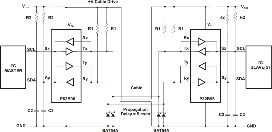 Figure 10. Driving Ribbon or Flat Telephone Cables
10.2.1.1 Design Requirements
In this application, the P82B96 is used to drive a ribbon cable. The following are assumed to be true
- Sy/Sx side of I2C bus is at a known voltage from 3.3 V to 5 V
- Tx/Ty and Rx/Ry side of I2C bus is at a known voltage from 2 V to 15V
- SCL Clock Speed <= 400kHz
10.2.1.2 Detailed Design Procedure
Table 1. Bus Capabilities
| VCC1
(V) |
+V CABLE (V) |
VCC2
(V) |
R1 (Ω) |
R2 (kΩ) |
C2 (pF) |
CABLE LENGTH (m) |
CABLE CAPACITANCE | CABLE DELAY (ns) |
MASTER SCL PULSE DURATION (ns) |
BUS CLOCK SPEED (kHz) | MAXIMUM SLAVE RESPONSE DELAY | |
|---|---|---|---|---|---|---|---|---|---|---|---|---|
| HIGH | LOW | |||||||||||
| 5 | 12 | 5 | 750 | 2.2 | 400 | 250 | (1) | 1250 | 600 | 4000 | 120 | (2) |
| 5 | 12 | 5 | 750 | 2.2 | 220 | 100 | (1) | 500 | 600 | 2600 | 185 | (2) |
| 3.3 | 5 | 3.3 | 330 | 1 | 220 | 25 | 1 nF | 125 | 600 | 1500 | 390 | (2) |
| 3.3 | 5 | 3.3 | 330 | 1 | 100 | 3 | 120 pF | 15 | 600 | 1000 | 500 | 600 ns |
When the master SCL high and low periods can be programmed separately, the timings can allow for bus delays. The low period should be programmed to achieve the minimum 1300 ns plus the net delay in the slave response data signal caused by bus and buffer delays. The longest data delay is the sum of the delay of the falling edge of SCL from master to slave and the delay of the rising edge of SDA from slave data to master. The actual SCL frequency is lower than calculated from the programmed clock periods because the buffer stretches the programmed SCL low period. In the example for the 25-m cable in Table 1, the clock is stretched 400 ns, the falling edge of SCL is delayed 490 ns, and the SDA rising edge is delayed 570 ns. The required additional low period is (490 + 570) = 1060 ns and the I2C bus specifications already include an allowance for a worst-case bus rise time (0% to 70%) of 425 ns. The bus rise time can be 300 ns (30% to 70%), which means it can be 425 ns (0% to 70%). The 25-m cable delay times include all rise and fall times. Therefore, the device only needs to be programmed with an additional (1060 – 400 – 425) = 235 ns, making a total programmed low period 1535 ns. The programmed low is stretched by 400 ns to yield an actual bus low time of 1935 ns, which, allowing the minimum high period of 600 ns, yields a cycle period of 2535 ns or 394 kHz.
Note in both the 100-m and 250-m examples, the capacitive loading on the I2C buses at each end is within the maximum allowed Standard mode loading of 400 pF, but exceeds the Fast mode limit. This is an example of a hybrid mode, because it relies on the response delays of Fast mode parts, but uses (allowable) Standard mode bus loadings with rise times that contribute significantly to the system delays. The cables cause large propagation delays. Therefore, these systems must operate well below the 400-kHz limit, but illustrate how they still can exceed the 100-kHz limit, provided all parts are capable of Fast mode operation. The fastest example illustrates how the 400-kHz limit can be exceeded, provided master and slave parts have delay specifications smaller than the maximum allowed. Many TI slaves have delays shorter than 600 ns, but none have that specified.
10.2.1.3 Application Curve
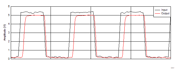 Figure 11. Propagation Delay Through P82B96 With 400-KHz Data
10.2.2 Galvanic Isolation
Figure 12 shows how the P82B96 can be used to galvanically isolate an I2C bus. This is achieved with the use of optocouplers to provide the isolation, and wiring the Rx/Ry and Tx/Ty pins to the appropriate diodes to allow for bidirectional operation.
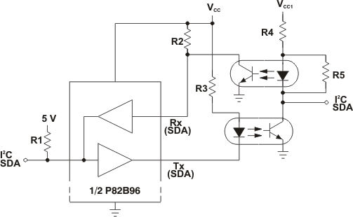 Figure 12. Galvanic Isolation of I2C Nodes
10.2.3 Long-Distance I2C
Figure 13 shows how the P82B96 can be used for long-distance I2C communications over a twisted pair. Tx and Rx share the same node and connect to one wire of a twisted pair, and Ty and Ry share the same node and connect to another twisted pair. One twisted pair should have 1 wire tied to VCC and the other twisted pair should have one of the wires tied to GND.
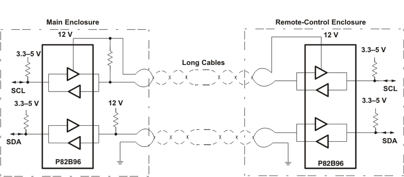 Figure 13. Long-Distance I2C Communications
10.2.4 Extend I2C/DDC Bus With Short-Circuit Protection
Figure 14 shows how a master I2C bus can be protected against short circuits or failures in applications that involve plug/socket connections and long cables that may become damaged. A simple circuit is added to monitor the SDA bus and, if its low time exceeds the design value, disconnect the master bus. P82B96 frees all of its I/Os if its supply is removed, so one option is to connect its VCC to the output of a logic gate from, for example, the LVC family. The SDA and SCL lines could be timed, and VCC disabled through the gate, if a line exceeds a design value of the low period. If the supply voltage of logic gates restricts the choice of VCC supply, the low-cost discrete circuit in Figure 14 can be used. If the SDA line is held low, the 100-nF capacitor charges, and Ry is pulled toward VCC. When it exceeds VCC/2, Ry sets Sy high, which effectively releases it.
In this example, the SCL line is made unidirectional by tying Rx to VCC. The state of the buffered SCL line cannot affect the master clock line, which is allowed when clock stretching is not required. It is simple to add an additional transistor or diode to control the Rx input in the same way as Ry, when necessary. The +V cable drive can be any voltage up to 15 V, and the bus may be run at a lower impedance by selecting pullup resistors for a static sink current up to 30 mA. VCC1 and VCC2 may be chosen to suit the connected devices. Because DDC uses relatively low speeds (<100 kHz), the cable length is not restricted to 20 m by the I2C signaling, but it may be limited by the video signaling.
Figure 10 and Table 1 show that P82B96 can achieve high clock rates over long cables. While calculating with lumped wiring capacitance yields reasonable approximations to actual timing; even 25 m of cable is better treated using transmission line theory. Flat ribbon cables connected as shown, with the bus signals on the outer edge, have a characteristic impedance in the range 100–200 Ω. For simplicity, they cannot be terminated in their characteristic impedance, but a practical compromise is to use the minimum pullup allowed for P82B96 and place half this termination at each end of the cable. When each pullup is less than 330 Ω, the rising-edge waveforms have their first voltage step level above the logic threshold at Rx, and cable timing calculations can be based on the fast rise/fall times of resistive loading, plus simple one-way propagation delays. When the pullup is larger, but less than 750 Ω, the threshold at Rx is crossed after one signal reflection. So, at the sending end, it is crossed after two times the one-way propagation delay and, at the receiving end, after three times that propagation delay. For flat cables with partial plastic dielectric insulation (by using outer cores) the one-way propagation delays are about 5 ns/m. The 10% to 90% rise and fall times on the cable are from 20 ns and 50 ns, so their delay contributions are small. There is ringing on falling edges that can be damped, if required, using Schottky diodes.
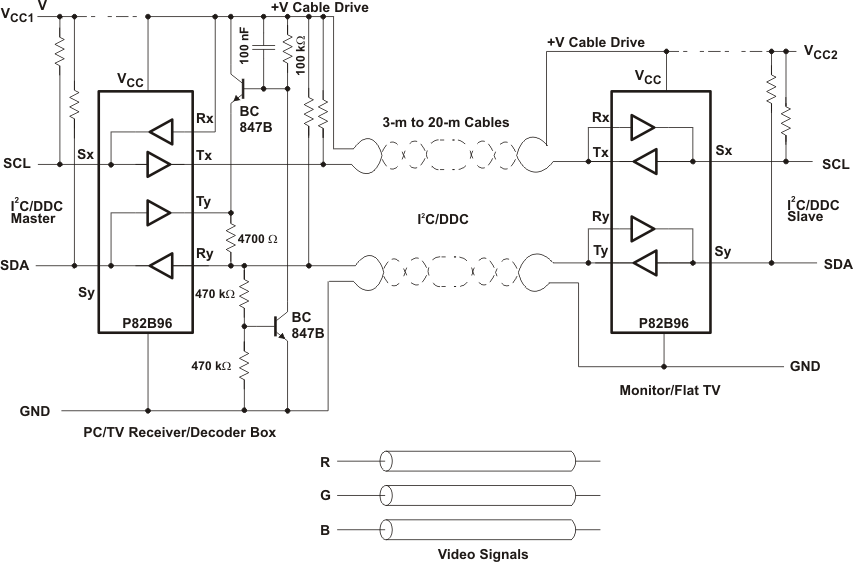 Figure 14. Extending DDC Bus
10.2.5 Voltage Translation
Figure 15 shows how the P82B96 can be used for I2C Voltage Translation.
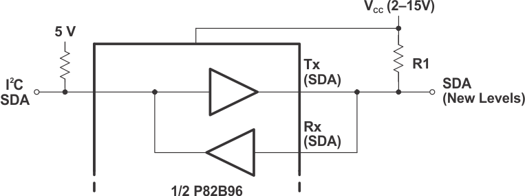 Figure 15. Interfacing I2C Bus With Different Logic Levels