SCPS144C May 2006 – May 2015 P82B96
PRODUCTION DATA.
- 1 Features
- 2 Applications
- 3 Description
- 4 Revision History
- 5 Description (continued)
- 6 Pin Configuration and Functions
-
7 Specifications
- 7.1 Absolute Maximum Ratings
- 7.2 ESD Ratings
- 7.3 Recommended Operating Conditions
- 7.4 Thermal Information
- 7.5 Electrical Characteristics: VCC = 2.3 V to 2.7 V
- 7.6 Electrical Characteristics: VCC = 3 V to 3.6 V
- 7.7 Electrical Characteristics: VCC = 4.5 V to 5.5 V
- 7.8 Electrical Characteristics: VCC = 15 V
- 7.9 Switching Characteristics
- 7.10 Typical Characteristics
- 8 Parameter Measurement Information
- 9 Detailed Description
- 10Application and Implementation
- 11Power Supply Recommendations
- 12Layout
- 13Device and Documentation Support
- 14Mechanical, Packaging, and Orderable Information
パッケージ・オプション
メカニカル・データ(パッケージ|ピン)
サーマルパッド・メカニカル・データ
発注情報
7 Specifications
7.1 Absolute Maximum Ratings
over operating free-air temperature range (unless otherwise noted)(1)| MIN | MAX | UNIT | |||
|---|---|---|---|---|---|
| VCC | Supply voltage on VCC pin | –0.3 | 18 | V | |
| VI | Voltage on buffered input | Sx or Sy (SDA or SCL) | –0.3 | 18 | V |
| Rx or Ry | –0.3 | 18 | |||
| VO | Voltage on buffered output | Sx or Sy (SDA or SCL) | –0.3 | 18 | V |
| Tx or Ty | –0.3 | 18 | |||
| IO | Continuous output current | Sx or Sy | 250 | mA | |
| Tx or Ty | 250 | ||||
| ICC | Continuous current through VCC or GND | 250 | mA | ||
| TA | Operating free-air temperature | –40 | 85 | °C | |
| Tstg | Storage temperature | –55 | 125 | °C | |
(1) Stresses beyond those listed under Absolute Maximum Ratings may cause permanent damage to the device. These are stress ratings only, and functional operation of the device at these or any other conditions beyond those indicated under Recommended Operating Conditions is not implied. Exposure to absolute-maximum-rated conditions for extended periods may affect device reliability.
7.2 ESD Ratings
| VALUE | UNIT | |||
|---|---|---|---|---|
| V(ESD) | Electrostatic discharge | Human Body Model (HBM), per ANSI/ESDA/JEDEC JS-001(1) | ±3500 | V |
| Charged-Device Model (CDM), per JEDEC specification JESD22-C101(2) | ±1000 | |||
| Machine Model (MM), per JEDEC specification JESD22-A115-A | ±200 | |||
(1) JEDEC document JEP155 states that 500-V HBM allows safe manufacturing with a standard ESD control process.
(2) JEDEC document JEP157 states that 250-V CDM allows safe manufacturing with a standard ESD control process.
7.3 Recommended Operating Conditions
| MIN | MAX | UNIT | ||||
|---|---|---|---|---|---|---|
| VCC | Supply voltage | 2 | 15 | V | ||
| IOL | Low-level output current | Sx, Sy | VSx, VSy = 1 V, VRx, VRy ≤ 0.42 V | 3 | mA | |
| Tx, Ty | VSx, VSy = 0.4 V, VTx, VTy = 0.4 V | 30 | ||||
| VIOmax | Maximum input/output voltage level | Sx, Sy | VTx, VTy = 0.4 V | 15 | V | |
| Tx, Ty | VSx, VSy = 0.4 V | 15 | ||||
| VILdiff | Low-level input voltage difference | Sx, Sy | 0.4 | V | ||
| TA | Operating free-air temperature | –40 | 85 | °C | ||
7.4 Thermal Information
| THERMAL METRIC(1) | P82B96 | UNIT | ||||
|---|---|---|---|---|---|---|
| D (SOIC) | DGK (VSSOP) | P (PDIP) | PW (TSSOP) | |||
| 8 PINS | 8 PINS | 8 PINS | 8 PINS | |||
| RθJA | Junction-to-ambient thermal resistance | 109.1 | 174.3 | 53.5 | 173.5 | °C/W |
| RθJC(top) | Junction-to-case (top) thermal resistance | 61.6 | 63 | 44.4 | 57.6 | °C/W |
| RθJB | Junction-to-board thermal resistance | 48.6 | 94.2 | 30.6 | 101.8 | °C/W |
| ψJT | Junction-to-top characterization parameter | 19.6 | 8.1 | 22.9 | 5.3 | °C/W |
| ψJB | Junction-to-board characterization parameter | 48.2 | 92.8 | 30.5 | 100.2 | °C/W |
(1) For more information about traditional and new thermal metrics, see the Semiconductor and IC Package Thermal Metrics application report, SPRA953.
7.5 Electrical Characteristics: VCC = 2.3 V to 2.7 V
VCC = 2.3 V to 2.7 V, voltages are specified with respect to GND (unless otherwise noted)| PARAMETER | TEST CONDITIONS |
TA = 25°C | TA = –40°C to 85°C | UNIT | ||||||
|---|---|---|---|---|---|---|---|---|---|---|
| MIN | TYP(1) | MAX | MIN | MAX | ||||||
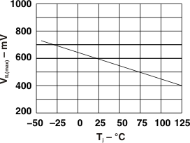
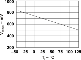
| ΔV/ΔTIN | Temperature coefficient of input thresholds | Sx, Sy | –2 | mV/°C | ||||||
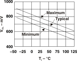
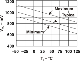
| VOL | Low-level output voltage | Sx, Sy | ISx, ISy = 3 mA | 0.8 | 0.88 | 1 | See (2) | V | ||
| ISx, ISy = 0.2 mA | 0.67 | 0.73 | 0.79 | See (2) | ||||||
| ΔV/ΔTOUT | Temperature coefficient of output low levels(3) | Sx, Sy | ISx, ISy = 0.2 mA | –1.8 | mV/°C | |||||
| ICC | Quiescent supply current | Sx = Sy = VCC | 0.9 | 1.8 | 2 | mA | ||||
| ΔICC | Additional supply current per pin low | Tx, Ty | 1.7 | 2.75 | 3 | mA | ||||
| IIOS | Dynamic output sink capability on I2C bus | Sx, Sy | VSx, VSy > 2 V, VRx, VRy = low | 7 | 18 | 5.5 | mA | |||
| Leakage current on I2C bus | VSx, VSy = 2.5 V, VRx, VRy = high | 0.1 | 1 | 1 | μA | |||||
| IIOT | Dynamic output sink capability on buffered bus | Tx, Ty | VTx, VTy > 1 V, VSx, VSy = low on I2C bus = 0.4 V |
60 | 100 | 60 | mA | |||
| Leakage current on buffered bus | VTx, VTy = VCC = 2.5 V, VSx, VSy = high | 0.1 | 1 | 1 | μA | |||||
| II | Input current from I2C bus | Sx, Sy | Bus low, VRx, VRy = high | –1 | 1 | μA | ||||
| Input current from buffered bus | Rx, Ry | Bus low, VRx, VRy = 0.4 V | –1 | 1 | ||||||
| Leakage current on buffered bus input | VRx, VRy = VCC | 1 | 1.5 | |||||||
| VIT | Input threshold | Sx, Sy | Input logic level high threshold(4) on normal I2C bus | 0.65 | 0.7 | See (2) | V | |||
| Input logic level low threshold(4) on normal I2C bus | 0.6 | 0.65 | See (2) | |||||||
| Rx, Ry | Input logic level high | 0.58 x VCC | 0.58 x VCC | |||||||
| Input threshold | 0.5 x VCC | |||||||||
| Input logic level low | 0.42 x VCC | 0.42 x VCC | ||||||||
| VIOdiff | Input/output logic level difference(5) | Sx, Sy | (VSx output low at 3 mA) – (VSx input high max) for I2C applications | 100 | 150 | 100 | mV | |||
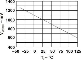
| VIOrel | VCC voltage at which all buses are released | Sx, Sy Tx, Ty |
Sx, Sy are low, VCC ramping, voltage on Tx, Ty lowered until released | 1 | 1 | V | ||||
| ΔV/ΔTREL | Temperature coefficient of release voltage | –4 | mV/°C | |||||||
| Cin | Input capacitance | Rx, Ry | 2.5 | 4 | 4 | pF | ||||
(1) Typical value is at VCC = 2.5 V, TA = 25°C
(2) See the Typical Characteristics section of this data sheet.
(3) The output logic low depends on the sink current.
(4) The input logic threshold is independent of the supply voltage.
(5) The minimum value requirement for pullup current, 200 μA, ensures that the minimum value for VSX output low always exceeds the minimum VSx input high level to eliminate any possibility of latching. The specified difference is specified by design within any device. While the tolerances on absolute levels allow a small probability that the low from one Sx output is recognized by an Sx input of another P82B96, this has no consequences for normal applications.
7.6 Electrical Characteristics: VCC = 3 V to 3.6 V
VCC = 3 V to 3.6 V, voltages are specified with respect to GND (unless otherwise noted)| PARAMETER | TEST CONDITIONS | TA = 25°C | TA = –40°C to 85°C | UNIT | |||||
|---|---|---|---|---|---|---|---|---|---|
| MIN | TYP(1) | MAX | MIN | MAX | |||||
| ΔV/ΔTIN | Temperature coefficient of input thresholds | Sx, Sy | –2 | mV/°C | |||||
| VOL | Low-level output voltage | Sx, Sy | ISx, ISy = 3 mA | 0.8 | 0.88 | 1 | See (2) | V | |
| ISx, ISy = 0.2 mA | 0.67 | 0.73 | 0.79 | See (2) | |||||
| ΔV/ΔTOUT | Temperature coefficient of output low levels(3) | Sx, Sy | ISx, ISy = 0.2 mA | –1.8 | mV/°C | ||||
| ICC | Quiescent supply current | Sx = Sy = VCC | 0.9 | 1.8 | 2 | mA | |||
| ΔICC | Additional supply current per pin low | Tx, Ty | 1.7 | 2.75 | 3 | mA | |||
| IIOS | Dynamic output sink capability on I2C bus | Sx, Sy | VSx, VSy > 2 V, VRx, VRy = low | 7 | 18 | 5.7 | mA | ||
| Leakage current on I2C bus | VSx, VSy = 5 V, VRx, VRy = high | 0.1 | 1 | 1 | μA | ||||
| IIOT | Dynamic output sink capability on buffered bus | Tx, Ty | VTx, VTy > 1 V, VSx, VSy = low on I2C bus = 0.4 V |
60 | 100 | 60 | mA | ||
| Leakage current on buffered bus | VTx, VTy = VCC = 3.3 V, VSx, VSy = high | 0.1 | 1 | 1 | μA | ||||
| II | Input current from I2C bus | Sx, Sy | Bus low, VRx, VRy = high | –1 | 1 | μA | |||
| Input current from buffered bus | Rx, Ry | Bus low, VRx, VRy = 0.4 V | –1 | 1 | |||||
| Leakage current on buffered bus input |
VRx, VRy = VCC | 1 | 1.5 | ||||||
| VIT | Input threshold | Sx, Sy | Input logic-level high threshold(4) on normal I2C bus | 0.65 | 0.7 | See (2) | V | ||
| Input logic-level low threshold(4) on normal I2C bus | 0.6 | 0.65 | See (2) | ||||||
| Rx, Ry | Input logic level high | 0.58 x VCC | 0.58 x VCC | ||||||
| Input threshold | 0.5 x VCC | ||||||||
| Input logic level low | 0.42 x VCC | 0.42 x VCC | |||||||
| VIOdiff | Input/output logic level difference(4) | Sx, Sy | (VSx output low at 3 mA) – (VSx input high max) for I2C applications | 100 | 150 | 100 | mV | ||
| VIOrel | VCC voltage at which all buses are released | Sx, Sy Tx, Ty |
Sx, Sy are low, VCC ramping, voltage on Tx, Ty lowered until released | 1 | 1 | V | |||
| ΔV/ΔTREL | Temperature coefficient of release voltage | –4 | mV/°C | ||||||
| Cin | Input capacitance | Rx, Ry | 2.5 | 4 | 4 | pF | |||
(1) Typical value is at VCC = 3.3 V, TA = 25°C
(2) See the Typical Characteristics section of this data sheet.
(3) The output logic low depends on the sink current.
(4) The minimum value requirement for pullup current, 200 μA, ensures that the minimum value for VSX output low always exceeds the minimum VSx input high level to eliminate any possibility of latching. The specified difference is specified by design within any device. While the tolerances on absolute levels allow a small probability that the low from one Sx output is recognized by an Sx input of another P82B96, this has no consequences for normal applications.
7.7 Electrical Characteristics: VCC = 4.5 V to 5.5 V
VCC = 4.5 V to 5.5 V, voltages are specified with respect to GND (unless otherwise noted)| PARAMETER | TEST CONDITIONS | TA = 25°C | TA = –40°C to 85°C | UNIT | |||||
|---|---|---|---|---|---|---|---|---|---|
| MIN | TYP(4) | MAX | MIN | MAX | |||||
| ΔV/ΔTIN | Temperature coefficient of input thresholds | Sx, Sy | –2 | mV/°C | |||||
| VOL | Low-level output voltage | Sx, Sy | ISx, ISy = 3 mA | 0.8 | 0.88 | 1 | See (5) | V | |
| ISx, ISy = 0.2 mA | 0.67 | 0.73 | 0.79 | See (5) | |||||
| ΔV/ΔTOUT | Temperature coefficient of output low levels(2) | Sx, Sy | ISx, ISy = 0.2 mA | –1.8 | mV/°C | ||||
| ICC | Quiescent supply current | Sx = Sy = VCC | 0.9 | 1.8 | 2 | mA | |||
| ΔICC | Additional supply current per pin low | Tx, Ty | 1.7 | 2.75 | 3 | mA | |||
| IIOS | Dynamic output sink capability on I2C bus | Sx, Sy | VSx, VSy > 2 V, VRx, VRy = low | 7 | 18 | 6 | mA | ||
| Leakage current on I2C bus | VSx, VSy = 5 V, VRx, VRy = high | 0.1 | 1 | 1 | μA | ||||
| IIOT | Dynamic output sink capability on buffered bus | Tx, Ty | VTx, VTy > 1 V, VSx, VSy = low on I2C bus = 0.4 V |
60 | 100 | 60 | mA | ||
| Leakage current on buffered bus | VTx, VTy = VCC = 5 V, VSx, VSy = high | 0.1 | 1 | 1 | μA | ||||
| II | Input current from I2C bus | Sx, Sy | Bus low, VRx, VRy = high | –1 | 1 | μA | |||
| Input current from buffered bus | Rx, Ry | Bus low, VRx, VRy = 0.4 V | –1 | 1 | |||||
| Leakage current on buffered bus input |
VRx, VRy = VCC | 1 | 1.5 | ||||||
| VIT | Input threshold | Sx, Sy | Input logic-level high threshold(3) on normal I2C bus | 0.65 | 0.7 | See (5) | V | ||
| Input logic-level low threshold(3) on normal I2C bus | 0.6 | 0.65 | See (5) | ||||||
| Rx, Ry | Input logic level high | 0.58 x VCC | 0.58 x VCC | ||||||
| Input threshold | 0.5 x VCC | ||||||||
| Input logic level low | 0.42 x VCC | 0.42 x VCC | |||||||
| VIOdiff | Input/output logic level difference(1) | Sx, Sy | (VSx output low at 3 mA) – (VSx input high max) for I2C applications | 100 | 150 | 100 | mV | ||
| VIOrel | VCC voltage at which all buses are released | Sx, Sy Tx, Ty |
Sx, Sy are low, VCC ramping, voltage on Tx, Ty lowered until released | 1 | 1 | V | |||
| ΔV/ΔTREL | Temperature coefficient of release voltage | –4 | mV/°C | ||||||
| Cin | Input capacitance | Rx, Ry | 2.5 | 4 | 4 | pF | |||
(1) The minimum value requirement for pullup current, 200 μA, ensures that the minimum value for VSX output low always exceeds the minimum VSx input high level to eliminate any possibility of latching. The specified difference is specified by design within any device. While the tolerances on absolute levels allow a small probability that the low from one Sx output is recognized by an Sx input of another P82B96, this has no consequences for normal applications.
(2) The output logic low depends on the sink current.
(3) The input logic threshold is independent of the supply voltage.
(4) Typical value is at VCC = 5 V, TA = 25°C
(5) See the Typical Characteristics section of this data sheet.
7.8 Electrical Characteristics: VCC = 15 V
VCC = 15 V, voltages are specified with respect to GND (unless otherwise noted)| PARAMETER | TEST CONDITIONS | TA = 25°C | TA = –40°C to 85°C | UNIT | |||||
|---|---|---|---|---|---|---|---|---|---|
| MIN | TYP(4) | MAX | MIN | MAX | |||||
| ΔV/ΔTIN | Temperature coefficient of input thresholds | Sx, Sy | –2 | mV/°C | |||||
| VOL | Low-level output voltage | Sx, Sy | ISx, ISy = 3 mA | 0.8 | 0.88 | 1 | See (5) | V | |
| ISx, ISy = 0.2 mA | 0.67 | 0.73 | 0.79 | See (5) | |||||
| ΔV/ΔTOUT | Temperature coefficient of output low levels(2) | Sx, Sy | ISx, ISy = 0.2 mA | –1.8 | mV/°C | ||||
| ICC | Quiescent supply current | Sx = Sy = VCC | 0.9 | 1.8 | 2 | mA | |||
| ΔICC | Additional supply current per pin low | Tx, Ty | 1.7 | 2.75 | 3 | mA | |||
| IIOS | Dynamic output sink capability on I2C bus | Sx, Sy | VSx, VSy > 2 V, VRx, VRy = low | 7 | 18 | 6.5 | mA | ||
| Leakage current on I2C bus | VSx, VSy = 15 V, VRx, VRy = high | 0.1 | 1 | 1 | μA | ||||
| IIOT | Dynamic output sink capability on buffered bus | Tx, Ty | VTx, VTy > 1 V, VSx, VSy = low on I2C bus = 0.4 V |
60 | 100 | 60 | mA | ||
| Leakage current on buffered bus | VTx, VTy = VCC = 15 V, VSx, VSy = high | 0.1 | 1 | 1 | μA | ||||
| II | Input current from I2C bus | Sx, Sy | Bus low, VRx, VRy = high | –1 | 1 | μA | |||
| Input current from buffered bus | Rx, Ry | Bus low, VRx, VRy = 0.4 V | –1 | 1 | |||||
| Leakage current on buffered bus input |
VRx, VRy = VCC | 1 | 1.5 | ||||||
| VIT | Input threshold | Sx, Sy | Input logic-level high threshold(3) on normal I2C bus | 0.65 | 0.7 | See (5) | V | ||
| Input logic-level high threshold(3) on normal I2C bus | 0.6 | 0.65 | See (5) | ||||||
| Rx, Ry | Input logic level high | 0.58 x VCC | 0.58 x VCC | ||||||
| Input threshold | 0.5 x VCC | ||||||||
| Input logic level low | 0.42 x VCC | 0.42 x VCC | |||||||
| VIOdiff | Input/output logic level difference(1) | Sx, Sy | (VSx output low at 3 mA) – (VSx input high max) for I2C applications | 100 | 150 | 100 | mV | ||
| VIOrel | VCC voltage at which all buses are released | Sx, Sy Tx, Ty |
Sx, Sy are low, VCC ramping, voltage on Tx, Ty lowered until released | 1 | 1 | V | |||
| ΔV/ΔTREL | Temperature coefficient of release voltage | –4 | mV/°C | ||||||
| Cin | Input capacitance | Rx, Ry | 2.5 | 4 | 4 | pF | |||
(1) The minimum value requirement for pullup current, 200 μA, ensures that the minimum value for VSX output low always exceeds the minimum VSx input high level to eliminate any possibility of latching. The specified difference is specified by design within any device. While the tolerances on absolute levels allow a small probability that the low from one Sx output is recognized by an Sx input of another P82B96, this has no consequences for normal applications.
(2) The output logic low depends on the sink current.
(3) The input logic threshold is independent of the supply voltage.
(4) Typical value is at VCC = 15 V, TA = 25°C
(5) See the Typical Characteristics section of this data sheet.
7.9 Switching Characteristics
VCC = 5 V, TA = 25°C, no capacitive loads, voltages are specified with respect to GND (unless otherwise noted)| PARAMETER | FROM (INPUT) |
TO (OUTPUT) |
TEST CONDITIONS | TYP | UNIT | |
|---|---|---|---|---|---|---|
| tpzl | Buffer delay time on falling input | VSx (or VSy) = input switching threshold | VTx (or VTy) output falling 50% of VLOAD(1) | RTx pullup = 160 Ω, CTx = 7 pF + board trace capacitance | 70 | ns |
| tplz | Buffer delay time on rising input | VSx (or VSy) = input switching threshold | VTx (or VTy) output reaching 50% of VLOAD(3) | RTx pullup = 160 Ω, CTx = 7 pF + board trace capacitance | 90 | ns |
| tpzl | Buffer delay time on falling input | VRx (or VRy) = input switching threshold | VSx (or VSy) output falling 50% of VLOAD(2) | RSx pullup = 1500 Ω, CTx = 7 pF + board trace capacitance | 250 | ns |
| tplz | Buffer delay time on rising input | VRx (or VRy) = input switching threshold | VSx (or VSy) output reaching 50% of VLOAD(4) | RSx pullup = 1500 Ω, CTx = 7 pF + board trace capacitance | 270 | ns |
(1) The fall time of VTx from 5 V to 2.5 V in the test is approximately 15 ns.
(2) The fall time of VSx from 5 V to 2.5 V in the test is approximately 50 ns.
(3) The rise time of VTx from 0 V to 2.5 V in the test is approximately 20 ns.
(4) The rise time of VSx from 0.9 V to 2.5 V in the test is approximately 70 ns.
7.10 Typical Characteristics
