SCPS232B March 2012 – March 2016 PCA9515B
PRODUCTION DATA.
- 1 Features
- 2 Applications
- 3 Description
- 4 Revision History
- 5 Pin Configuration and Functions
- 6 Specifications
- 7 Parameter Measurement Information
- 8 Detailed Description
- 9 Application and Implementation
- 10Power Supply Recommendations
- 11Layout
- 12Device and Documentation Support
- 13Mechanical, Packaging, and Orderable Information
11 Layout
11.1 Layout Guidelines
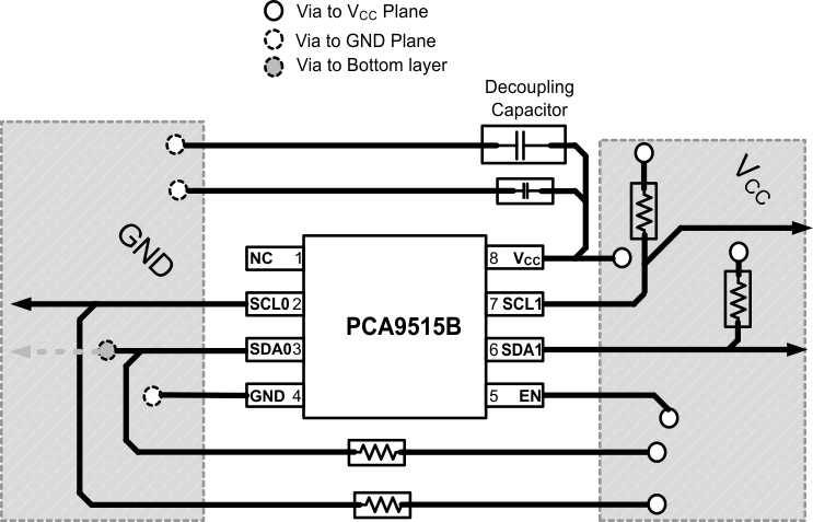
For printed circuit board (PCB) layout of the PCA9515B, common PCB layout practices should be followed. In all PCB layouts, it is a best practice to avoid right angles in signal traces, to fan out signal traces away from each other upon leaving the vicinity of an integrated circuit (IC), and to use thicker trace widths to carry higher amounts of current that commonly pass through power and ground traces. By-pass and de-coupling capacitors are commonly used to control the voltage on the VCC pin, using a larger capacitor to provide additional power in the event of a short power supply glitch and a small capacitor to filter out high-frequency ripple. These decoupling capacitors should be placed as close to the VCC pin of PCA9515B as possible.
The layout example shown in Figure 8 shows a 4 layer board, which is preferable for boards with higher density signal routing. On a 4 layer PCB, it is common to route signals on the top and bottom layer, dedicate one internal layer to a ground plane, and one to power plane. In a board layout using planes or split planes for power and ground, vias are placed directly next to the surface mount component pad which needs to attach to VCC or GND and the via is connected electrically to the internal layer on the other side of the board. Vias are also used when a signal trace needs to be routed to the opposite side of the board. This routing and via is not necessary if VCC and GND are both full planes as opposed to the partial planes depicted.
11.2 Layout Example
 Figure 8. Layout Schematic