SLASE12A July 2014 – October 2014 PCM5242
PRODUCTION DATA.
- 1 Features
- 2 Applications
- 3 Description
- 4 Simplified System Diagram
- 5 Revision History
- 6 Pin Configuration and Functions
- 7 Specifications
-
8 Detailed Description
- 8.1 Overview
- 8.2 Functional Block Diagram
- 8.3 Terminology
- 8.4 Audio Data Interface
- 8.5 XSMT Pin (Soft Mute / Soft Un-Mute)
- 8.6 Audio Processing
- 8.7 DAC and Differential Analog Outputs
- 8.8
Reset and System Clock Functions
- 8.8.1 Clocking Overview
- 8.8.2 Clock Slave Mode With Master Clock (SCK) Input (4 Wire I2S)
- 8.8.3 Clock Slave Mode with BCK PLL to Generate Internal Clocks (3-Wire PCM)
- 8.8.4 Clock Generation Using The PLL
- 8.8.5 PLL Calculation
- 8.8.6 Clock Master Mode from Audio Rate Master Clock
- 8.8.7 Clock Master from a Non-Audio Rate Master Clock
- 8.9 Device Functional Modes
- 9 Applications and Implementation
- 10Power Supply Recommendations
- 11Layout
-
12Programming and Registers Reference
- 12.1 Coefficient Data Formats
- 12.2
PCM5242 Register Map
- 12.2.1
Detailed Register Descriptions
- 12.2.1.1 Register Map Summary
- 12.2.1.2
Page 0 Registers
- 12.2.1.2.1 Page 0 / Register 1
- 12.2.1.2.2 Page 0 / Register 2
- 12.2.1.2.3 Page 0 / Register 3
- 12.2.1.2.4 Page 0 / Register 4
- 12.2.1.2.5 Page 0 / Register 6
- 12.2.1.2.6 Page 0 / Register 7
- 12.2.1.2.7 Page 0 / Register 8
- 12.2.1.2.8 Page 0 / Register 9
- 12.2.1.2.9 Page 0 / Register 10
- 12.2.1.2.10 Page 0 / Register 12
- 12.2.1.2.11 Page 0 / Register 13
- 12.2.1.2.12 Page 0 / Register 14
- 12.2.1.2.13 Page 0 / Register 18
- 12.2.1.2.14 Page 0 / Register 19
- 12.2.1.2.15 Page 0 / Register 20
- 12.2.1.2.16 Page 0 / Register 21
- 12.2.1.2.17 Page 0 / Register 22
- 12.2.1.2.18 Page 0 / Register 23
- 12.2.1.2.19 Page 0 / Register 24
- 12.2.1.2.20 Page 0 / Register 27
- 12.2.1.2.21 Page 0 / Register 28
- 12.2.1.2.22 Page 0 / Register 29
- 12.2.1.2.23 Page 0 / Register 30
- 12.2.1.2.24 Page 0 / Register 32
- 12.2.1.2.25 Page 0 / Register 33
- 12.2.1.2.26 Page 0 / Register 34
- 12.2.1.2.27 Page 0 / Register 35
- 12.2.1.2.28 Page 0 / Register 36
- 12.2.1.2.29 Page 0 / Register 37
- 12.2.1.2.30 Page 0 / Register 40
- 12.2.1.2.31 Page 0 / Register 41
- 12.2.1.2.32 Page 0 / Register 42
- 12.2.1.2.33 Page 0 / Register 43
- 12.2.1.2.34 Page 0 / Register 44
- 12.2.1.2.35 Page 0 / Register 59
- 12.2.1.2.36 Page 0 / Register 60
- 12.2.1.2.37 Page 0 / Register 61
- 12.2.1.2.38 Page 0 / Register 62
- 12.2.1.2.39 Page 0 / Register 63
- 12.2.1.2.40 Page 0 / Register 64
- 12.2.1.2.41 Page 0 / Register 65
- 12.2.1.2.42 Page 0 / Register 80
- 12.2.1.2.43 Page 0 / Register 81
- 12.2.1.2.44 Page 0 / Register 82
- 12.2.1.2.45 Page 0 / Register 83
- 12.2.1.2.46 Page 0 / Register 84
- 12.2.1.2.47 Page 0 / Register 85
- 12.2.1.2.48 Page 0 / Register 86
- 12.2.1.2.49 Page 0 / Register 87
- 12.2.1.2.50 Page 0 / Register 90
- 12.2.1.2.51 Page 0 / Register 91
- 12.2.1.2.52 Page 0 / Register 92
- 12.2.1.2.53 Page 0 / Register 93
- 12.2.1.2.54 Page 0 / Register 94
- 12.2.1.2.55 Page 0 / Register 95
- 12.2.1.2.56 Page 0 / Register 108
- 12.2.1.2.57 Page 0 / Register 109
- 12.2.1.2.58 Page 0 / Register 114
- 12.2.1.2.59 Page 0 / Register 115
- 12.2.1.2.60 Page 0 / Register 118
- 12.2.1.2.61 Page 0 / Register 119
- 12.2.1.2.62 Page 0 / Register 120
- 12.2.1.2.63 Page 0 / Register 121
- 12.2.1.2.64 Page 0 / Register 122
- 12.2.1.2.65 Page 0 / Register 123
- 12.2.1.2.66 Page 0 / Register 124
- 12.2.1.2.67 Page 0 / Register 125
- 12.2.1.3 Page 1 Registers
- 12.2.1.4 Page 44 Registers
- 12.2.1.5 Page 253 Registers
- 12.2.2 PLL Tables for Software Controlled Devices
- 12.2.1
Detailed Register Descriptions
- 13Device and Documentation Support
- 14Mechanical, Packaging, and Orderable Information
パッケージ・オプション
メカニカル・データ(パッケージ|ピン)
- RHB|32
サーマルパッド・メカニカル・データ
- RHB|32
発注情報
10 Power Supply Recommendations
10.1 Power Supply Distribution and Requirements
The PCM5242 is powered through the following pins:
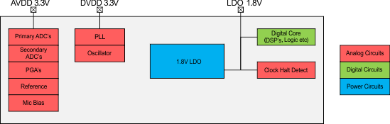 Figure 82. Power Distribution Tree within PCM5242
Table 45. Power Supply Pin Descriptions
| NAME | USAGE / DESCRIPTION |
|---|---|
| AVDD | Analog Voltage Supply - should be 3.3V. Powers the ADC, PGA, Reference, and Secondary ADC |
| DVDD | Digital Voltage Supply - This is used as the I/O voltage control and the input to the onchip LDO. |
| CPVDD | Charge Pump Voltage Supply - should be 3.3V |
| LDOO | Output from the Onchip LDO. Should be used with a 0.1uF decoupling cap. Can be driven (used as power input) with a 1.8V supply to bypass the onchip LDO for lower power consumption. |
| AGND | Analog Ground |
| DGND | Digital Ground |
10.2 Recommended Powerdown Sequence
Under certain conditions, the PCM5242 can exhibit some pop on power down. Pops are caused by the device not having enough time to detect power loss and start the muting process.
The PCM5242 has two auto-mute functions to mute the device upon power loss (intentional or unintentional).
XSMT = 0
When the XSMT pin is pulled low, the incoming PCM data is attenuated to 0, closely followed by a hard analog mute. This process takes 150 sample times (ts) + 0.2mS.
Because this mute time is mainly dominated by the sampling frequency, systems sampling at 192kHz will mute much faster than a 48kHz system.
Clock Error Detect
When clock error is detected on the incoming data clock, the PCM5242 switches to an internal oscillator, and continues to the drive the output, while attenuating the data from the last known value. Once this process is complete, the PCM5242 outputs are hard muted to ground.
10.2.1 Planned Shutdown
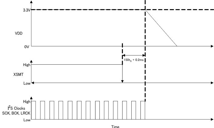
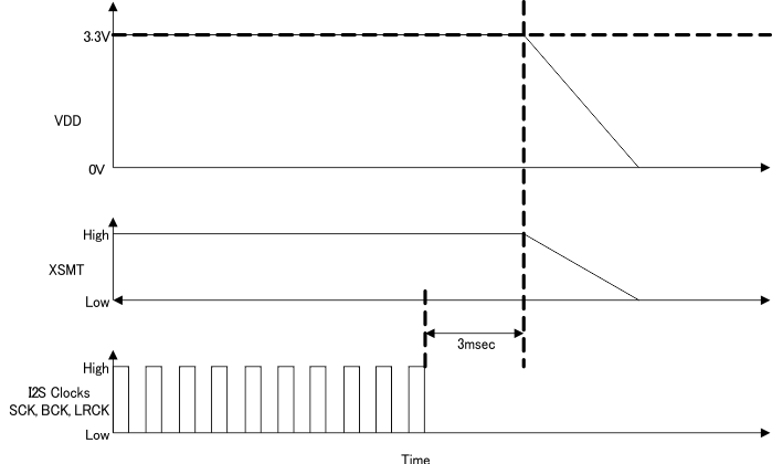
These auto-muting processes can be manipulated by system designs to mute before power loss in the following ways:
- Assert XSMT low 150tS + 0.2mS before power is removed.
- Stop I2S clocks (SCK, BCK, LRCK) 3ms before powerdown as shown below:
10.2.2 Unplanned Shutdown
Many systems use a low-noise regulator to provide an AVDD 3.3V supply for the DAC. The XSMT Pin can take advantage of such a feature to measure the pre-regulated output from the system SMPS to mute the output before the entire SMPS discharges. Figure 83 shows how to configure such a system to use the XSMT pin. The XSMT pin can also be used in parallel with a GPIO pin from the system microcontroller/DSP or Power Supply.
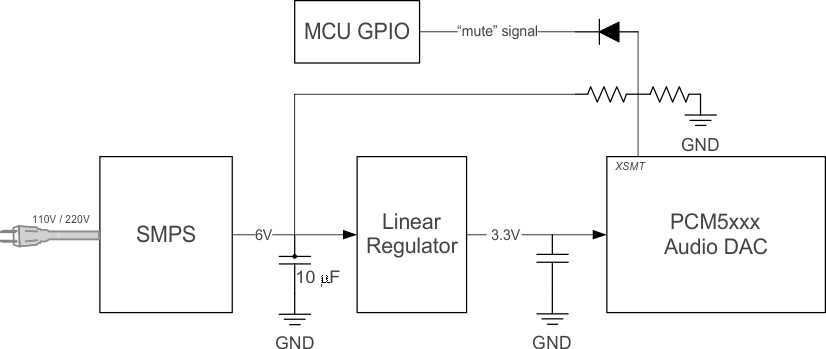 Figure 83. Using the XSMT Pin
10.3 External Power Sense Undervoltage Protection mode (supported only when DVDD = 3.3V)
The XSMT pin can also be used to monitor a system voltage, such as the 24VDC LCD TV backlight, or 12VDC system supply using a voltage divider created with two resistors. (See Figure 84 )
- If the XSMT pin makes a transition from “1” to “0” over 6ms or more, the device switches into external under-voltage protection mode. This mode uses two trigger levels.
- When the XSMT pin level reaches 2V, soft mute process begins.
- When the XSMT pin level reaches 1.2V, analog mute engages, regardless of digital audio level, and analog shutdown begins. (DAC and related circuitry powers down).
A timing diagram to show this is shown in Figure 85.
NOTE
The XSMT input pin voltage range is from -0.3V to DVDD + 0.3V.The ratio of external resistors must produce a voltage within this input range. Any increase in power supply (such as power supply positive noise or ripple) can pull the XSMT pin higher than DVDD+0.3V.
For example, if the PCM5242 is monitoring a 12V input, and dividing the voltage by 4, then the voltage at XSMT during ideal power supply conditions is 3V. A voltage spike higher than 14.4V causes a voltage greater than 3.6V (DVDD+0.3) on the XSMT pin, potentially damaging the device.
Providing the divider is set appropriately, any DC voltage can be monitored.
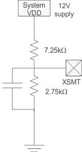 Figure 84. XSMT in External UVP Mode
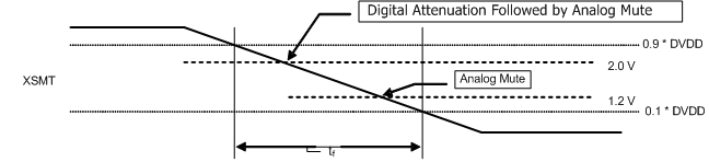 Figure 85. XSMT Timing for Undervoltage Protection
Power-On Reset Function
Power-On Reset, DVDD 3.3V Supply
The PCM5242 includes a power-on reset function shown in Figure 86. With VDD > 2.8V, the power-on reset function is enabled. After the initialization period, the PCM5242 is set to its default reset state.
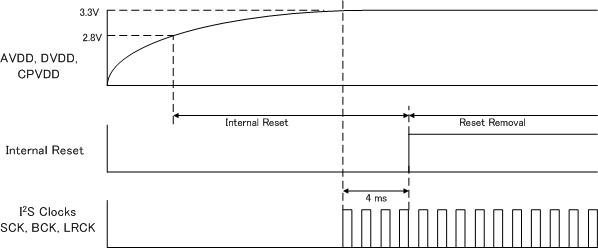 Figure 86. Power-On Reset Timing, DVDD = 3.3V
Power-On Reset, DVDD 1.8V Supply
The PCM5242 includes a power-on reset function shown in Figure 87 operating at DVDD=1.8V. With AVDD greater than approximately 2.8V, CPVDD greater than approximately 2.8V, and DVDD greater than approximately 1.5V, the power-on reset function is enabled. After the initialization period, the PCM5242 is set to its default reset state.
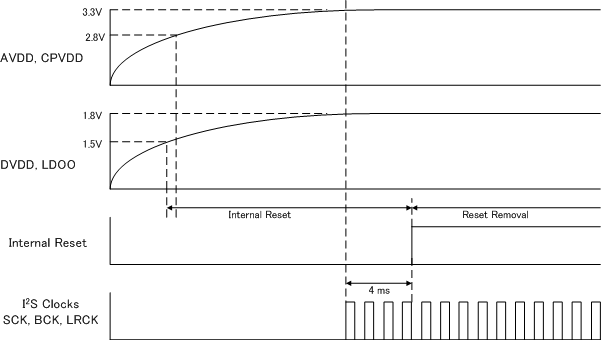 Figure 87. Power-On Reset Timing, DVDD = 1.8V
10.4 PCM5242 Power Modes
10.4.1 Setting Digital Power Supplies and I/O Voltage Rails
The internal digital core of the PCM5242 runs from a 1.8V supply. This can be generated by the internal LDO, or by an external 1.8V supply.
DVDD is used to set the I/O voltage, and to be used as the input to the onchip LDO that creates the 1.8V required by the digital core.
For systems that require 3.3V IO support, but lower power consumption, DVDD should be connected to 3.3V and LDOO can be connected to an external 1.8V source. Doing so will disable the onchip LDO.
When setting IO voltage to be 1.8V, both DVDD and LDOO must be provided with an external 1.8V supply.
10.4.2 Power Save Modes
The PCM5242 offers two power-save modes; standby and power-down.
When a clock error (SCK, BCK, and LRCK) or clock halt is detected, the PCM5242 automatically enters standby mode. The DAC and line driver are also powered down. The device can also be placed in standby mode via software command.
When BCK and LRCK remain at a low level for more than 1 second, the PCM5242 automatically enters power-down mode. Power-down mode disables the negative charge pump and bias/reference circuit, in addition to those disabled in standby mode. The device can also be placed in power-down mode via software command.
The detection time of BCK and LRCK halt can be controlled by Page 0, Register 44, D(2:0).
When expected Audio clocks (SCK, BCK, LRCK) are applied to the PCM5242, the device starts its powerup sequence automatically. The detection time for BCK and LRCK halt is programmable.
10.4.3 Power Save Parameter Programming
| Register | Description |
|---|---|
| Page 0, Register 2, D(4) | Software standby mode command |
| Page 0, Register 2, D(0) | Software power-down command |
| Page 0, Register 2, D(4) and D(0) | Software power-up sequence command (required after software standby or power-down) |
| Page 0, Register 44, D(2:0) | Detection time of BCK and LRCK halt |