SLASE12A July 2014 – October 2014 PCM5242
PRODUCTION DATA.
- 1 Features
- 2 Applications
- 3 Description
- 4 Simplified System Diagram
- 5 Revision History
- 6 Pin Configuration and Functions
- 7 Specifications
-
8 Detailed Description
- 8.1 Overview
- 8.2 Functional Block Diagram
- 8.3 Terminology
- 8.4 Audio Data Interface
- 8.5 XSMT Pin (Soft Mute / Soft Un-Mute)
- 8.6 Audio Processing
- 8.7 DAC and Differential Analog Outputs
- 8.8
Reset and System Clock Functions
- 8.8.1 Clocking Overview
- 8.8.2 Clock Slave Mode With Master Clock (SCK) Input (4 Wire I2S)
- 8.8.3 Clock Slave Mode with BCK PLL to Generate Internal Clocks (3-Wire PCM)
- 8.8.4 Clock Generation Using The PLL
- 8.8.5 PLL Calculation
- 8.8.6 Clock Master Mode from Audio Rate Master Clock
- 8.8.7 Clock Master from a Non-Audio Rate Master Clock
- 8.9 Device Functional Modes
- 9 Applications and Implementation
- 10Power Supply Recommendations
- 11Layout
-
12Programming and Registers Reference
- 12.1 Coefficient Data Formats
- 12.2
PCM5242 Register Map
- 12.2.1
Detailed Register Descriptions
- 12.2.1.1 Register Map Summary
- 12.2.1.2
Page 0 Registers
- 12.2.1.2.1 Page 0 / Register 1
- 12.2.1.2.2 Page 0 / Register 2
- 12.2.1.2.3 Page 0 / Register 3
- 12.2.1.2.4 Page 0 / Register 4
- 12.2.1.2.5 Page 0 / Register 6
- 12.2.1.2.6 Page 0 / Register 7
- 12.2.1.2.7 Page 0 / Register 8
- 12.2.1.2.8 Page 0 / Register 9
- 12.2.1.2.9 Page 0 / Register 10
- 12.2.1.2.10 Page 0 / Register 12
- 12.2.1.2.11 Page 0 / Register 13
- 12.2.1.2.12 Page 0 / Register 14
- 12.2.1.2.13 Page 0 / Register 18
- 12.2.1.2.14 Page 0 / Register 19
- 12.2.1.2.15 Page 0 / Register 20
- 12.2.1.2.16 Page 0 / Register 21
- 12.2.1.2.17 Page 0 / Register 22
- 12.2.1.2.18 Page 0 / Register 23
- 12.2.1.2.19 Page 0 / Register 24
- 12.2.1.2.20 Page 0 / Register 27
- 12.2.1.2.21 Page 0 / Register 28
- 12.2.1.2.22 Page 0 / Register 29
- 12.2.1.2.23 Page 0 / Register 30
- 12.2.1.2.24 Page 0 / Register 32
- 12.2.1.2.25 Page 0 / Register 33
- 12.2.1.2.26 Page 0 / Register 34
- 12.2.1.2.27 Page 0 / Register 35
- 12.2.1.2.28 Page 0 / Register 36
- 12.2.1.2.29 Page 0 / Register 37
- 12.2.1.2.30 Page 0 / Register 40
- 12.2.1.2.31 Page 0 / Register 41
- 12.2.1.2.32 Page 0 / Register 42
- 12.2.1.2.33 Page 0 / Register 43
- 12.2.1.2.34 Page 0 / Register 44
- 12.2.1.2.35 Page 0 / Register 59
- 12.2.1.2.36 Page 0 / Register 60
- 12.2.1.2.37 Page 0 / Register 61
- 12.2.1.2.38 Page 0 / Register 62
- 12.2.1.2.39 Page 0 / Register 63
- 12.2.1.2.40 Page 0 / Register 64
- 12.2.1.2.41 Page 0 / Register 65
- 12.2.1.2.42 Page 0 / Register 80
- 12.2.1.2.43 Page 0 / Register 81
- 12.2.1.2.44 Page 0 / Register 82
- 12.2.1.2.45 Page 0 / Register 83
- 12.2.1.2.46 Page 0 / Register 84
- 12.2.1.2.47 Page 0 / Register 85
- 12.2.1.2.48 Page 0 / Register 86
- 12.2.1.2.49 Page 0 / Register 87
- 12.2.1.2.50 Page 0 / Register 90
- 12.2.1.2.51 Page 0 / Register 91
- 12.2.1.2.52 Page 0 / Register 92
- 12.2.1.2.53 Page 0 / Register 93
- 12.2.1.2.54 Page 0 / Register 94
- 12.2.1.2.55 Page 0 / Register 95
- 12.2.1.2.56 Page 0 / Register 108
- 12.2.1.2.57 Page 0 / Register 109
- 12.2.1.2.58 Page 0 / Register 114
- 12.2.1.2.59 Page 0 / Register 115
- 12.2.1.2.60 Page 0 / Register 118
- 12.2.1.2.61 Page 0 / Register 119
- 12.2.1.2.62 Page 0 / Register 120
- 12.2.1.2.63 Page 0 / Register 121
- 12.2.1.2.64 Page 0 / Register 122
- 12.2.1.2.65 Page 0 / Register 123
- 12.2.1.2.66 Page 0 / Register 124
- 12.2.1.2.67 Page 0 / Register 125
- 12.2.1.3 Page 1 Registers
- 12.2.1.4 Page 44 Registers
- 12.2.1.5 Page 253 Registers
- 12.2.2 PLL Tables for Software Controlled Devices
- 12.2.1
Detailed Register Descriptions
- 13Device and Documentation Support
- 14Mechanical, Packaging, and Orderable Information
パッケージ・オプション
メカニカル・データ(パッケージ|ピン)
- RHB|32
サーマルパッド・メカニカル・データ
- RHB|32
発注情報
8 Detailed Description
8.1 Overview
The integrated PLL on the device provided adds the flexibility to remove the system clock (commonly known as master clock), allowing a 3-wire I2S connection and reducing system EMI. In addition, the PLL is completely programmable, allowing the device to become the I2S clock master and drive a DSP serial port as a slave. The PLL also accepts a non-standard clock (up to 50MHz) as a source to generate the audio related clock (for example 24.576MHz).
Powersense undervoltage protection utilizes a two-level mute system. Upon clock error or system power failure, the device digitally attenuates the data (or last known good data), then mutes the analog circuit.
Compared with existing DAC technology, the PCM5242 offers up to 20dB lower out-of-band noise, reducing EMI and aliasing in downstream amplifiers/ADCs. (from traditional 100kHz OBN measurements all the way to 3MHz).
The PCM5242 accepts industry-standard audio data formats with 16- to 32-bit data. Sample rates up to 384kHz are supported.
8.2 Functional Block Diagram

8.3 Terminology
Control registers in this datasheet are given by REGISTER BIT/BYTE NAME (Page.x HEX ADDRESS). SE refers to "Single Ended" analog inputs, DIFF refers to "Differential" analog inputs. SCK (System Clock) and MCLK (Master Clock) are used interchangeably. Sampling frequency is symbolized by "fS". Full scale is symbolized by "FS". Sample time as a unit is symbolized by "tS".
8.4 Audio Data Interface
8.4.1 Audio Serial Interface
The audio interface port is a 3-wire serial port with the signals LRCK, BCK, and DIN. BCK is the serial audio bit clock, used to clock the serial data present on DIN into the serial shift register of the audio interface. Serial data is clocked into the PCM5242 on the rising edge of BCK. LRCK is the serial audio left/right word clock. LRCK polarity for Left/Right is given by the format selected.
Table 4. PCM5242 Audio Data Formats, Bit Depths and Clock Rates
| CONTROL MODE | FORMAT | DATA BITS | MAX LRCK FREQUENCY [fS] | SCK RATE [x fS] | BCK RATE [x fS] |
|---|---|---|---|---|---|
| Software Control (SPI or I2S) |
I2S/LJ | 32, 24, 20, 16 | Up to 192kHz | 128 – 3072 | 64, 48, 32 |
| 384kHz | 64, 128 | 64, 48, 32 | |||
| TDM/DSP | 32, 24, 20, 16 | Up to 48kHz | 128 – 3072 | 125, 256 | |
| 96kHz | 128 – 512 | 125, 256 | |||
| 192kHz | 128, 192, 256 | 128 | |||
| Hardware Control | I2S/LJ | 32, 24, 20, 16 | Up to 192kHz | 128 – 3072 | 64, 48, 32 |
| 384kHz | 64, 128 | 64, 48, 32 |
The PCM5242 requires the synchronization of LRCK and system clock, but does not need a specific phase relation between LRCK and system clock.
If the relationship between LRCK and system clock changes more than ±5 SCK, internal operation is initialized within one sample period and analog outputs are forced to the bipolar zero level until resynchronization between LRCK and system clock is completed.
If the relationship between LRCK and BCK are invalid more than 4 LRCK periods, internal operation is initialized within one sample period and analog outputs are forced to the bipolar zero level until resynchronization between LRCK and BCK is completed.
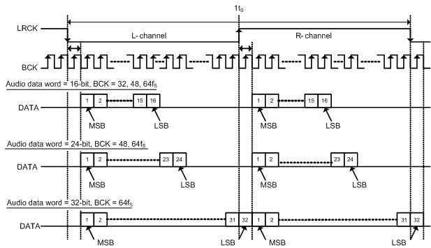
8.4.2 PCM Audio Data Formats
The PCM5242 supports industry-standard audio data formats, including standard I2S and left-justified. Data formats are selected via Register (Pg0Reg40). All formats require binary 2s-complement, MSB-first audio data; up to 32-bit audio data is accepted.
The PCM5242 also supports right-justified and TDM/DSP in software control mode. I2S, LJ, RJ, and TDM/DSP are selected using Register (Pg0Reg40). All formats require binary 2s complement, MSB-first audio data. Up to 32 bits are accepted. Default setting is I2S and 24 bit word length.
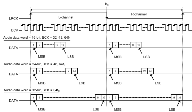 Figure 18. Left Justified Audio Data Format
The following data formats are only available in software mode.
NOTE
In TDM Modes, Duty Cycle of LRCK should be 1x BCK at minimum. Rising edge is considered frame start.
8.4.3 Zero Data Detect
The PCM5242 has a zero-detect function. When the device detects the continuous zero data for both left and right channels, or separate channels, Analog mutes are set to both OUTL and OUTR, or separate OUTL and OUTR. These are controlled by Page0, Register 65, D(2:1) as shown in Table 5.
Continuous Zero data cycles are counted by LRCK, and the threshold of decision for analog mute can be set by Page 0, Register 59, D(6:4) for L-ch, and D(2:0) for Rch as shown in Table 6. Default values are 0 for both channels.
In Hardware mode, the device uses default values.
Table 5. Zero Data Detection Mode
| ATMUTECTL | Value | Function |
| Bit : 2 | 0 | Independently L-ch or R-ch are zero data for zero data detection |
| 1 (Default) | Both L-ch and R-ch have to be zero data for zero data detection | |
| Bit : 1 | 0 | Zero detection and analog mute are disabled for R-ch |
| 1 (Default) | Zero detection analog mute are enabled for R-ch | |
| Bit : 0 | 0 | Zero detection analog mute are disabled for L-ch |
| 1 (Default) | Zero detection analog mute are enabled for L-ch |
Table 6. Zero Data Detection Time
| ATMUTETIML / ATMUTETIMR | Number of LRCKs | Time @ 48kHz |
| 0 0 0 | 1024 | 21 ms |
| 0 0 1 | 5120 | 106 ms |
| 0 1 0 | 10240 | 213 ms |
| 0 1 1 | 25600 | 533 ms |
| 1 0 0 | 51200 | 1.066 sec |
| 1 0 1 | 102400 | 2.133 sec |
| 1 1 0 | 256000 | 5.333 sec |
| 1 1 1 | 512000 | 10.66 sec |
8.5 XSMT Pin (Soft Mute / Soft Un-Mute)
An external digital host controls the PCM5242 soft mute function by driving the XSMT pin with a specific minimum rise time (tr) and fall time (tf) for soft mute and soft un-mute. The PCM5242 requires tr and tf times of less than 20ns. In the majority of applications, this is no problem, however, traces with high capacitance may have issues.
When the XSMT pin is shifted from high to low (3.3V to 0V), a soft digital attenuation ramp begins. -1dB attenuation is then applied every sample time from 0dBFS to - ∞. The soft attenuation ramp takes 104 samples.
When the XSMT pin is shifted from low to high (0V to 3.3V), a soft digital “un-mute” is started. 1dB gain steps are applied every sample time from - ∞ to 0dBFS. The un-mute takes 104 samples.
In systems where XSMT is not required, it can be directly connected to AVDD.
8.6 Audio Processing
8.6.1 PCM5242 Audio Processing Options
8.6.1.1 Overview
The PCM5242 features a fully-programmable miniDSP core. The algorithms for the miniDSP must be loaded into the device after power up. The miniDSP has direct access to the digital stereo audio stream, offering the possibility for advanced DSP algorithms with very low group delay. The miniDSP can run up to 1024 instructions on every audio sample at a 48kHz sample rate.
The PCM5242 features a programmable miniDSP core that offers Hybrid-Flows which are a RAM/ROM combination of code. Common functions are embedded in ROM, and custom RAM flows, created by TI can be run on the miniDSP core. The algorithms for the miniDSP must be loaded into the device after power up. The miniDSP can run up to 1024 instructions on every audio sample at a 48kHz sample rate. Development is done using Purepath Console software.
NOTE
At higher sampling frequencies, fewer instruction cycles are available. (For example, 512 instructions can be done in a 96kHz frame.)
The PCM5242 supports two different code sources. ROM based process flow (See the next section for how to select) and RAM based process flow. In program 31 (RAM based), different algorithms can be called from ROM - such as EQ, DRC and Zero Crossing volume control. Please see the PurePath Studio Development Environment for more details.
8.6.1.2 miniDSP Instruction Register
Registers on Page 152-169 are 25-bit instructions for the miniDSP engine. For details see Table 49. 7 bits of Instr(32:25) in Base register +0 are reserved bits. 1 bit of Instr(24) - (LSB) in Base register +0 is MSB bit of 25 bit instruction. These instructions control miniDSP operation. When the fully programmable miniDSP mode is enabled and the DAC channel is powered up, the read and write access to these registers is disabled.
8.6.1.3 Digital Output
The PCM5242 supports an SDOUT output. This can be selected within the process flow, and driven out of a GPIO pin selected in the register map (e.g. Page 0 / Register 80). Users should note that the I2S output will be attenuated by 0.5dB. A full scale (FS) output will actually be FS-0.5dB. This can be compensated for within the process flow using PurePath Studio. The I2S output can be a separate audio stream to the analog DAC output, allowing 2.1 and 2.2 systems to be implimented. By default, the SDOUT is not linked to the volume control registers on Page 0 / Register 60, 61, 62. However, it is possible to configure the SDOUT component in Purepath studio to mirror that register.
8.6.1.4 Software
Software development for the PCM5242 is supported through TI's comprehensive PurePath Console; a powerful, easy-to-use tool designed specifically to simplify software development on the PCM5242 miniDSP audio platform. The Graphical Development Environment consists of number of Hybrid Flows that can be downloaded to the device and run on the miniDSP.
Please visit the PCM5242 product folder on www.ti.com to learn more about PurePath Console and the latest status on available, ready-to-use DSP algorithms.
8.6.2 Interpolation Filter
The PCM5242 provides 4 types of interpolation filters, selectable by writing to Page 0, Register 43, D(4:0).
Additional RAM based Hybrid Flows can be implemented by selecting Program 31, and downloading instructions and coefficients to the device.
Table 7. ROM Preset Programs
| Program number | D(4:0) | Description | Minimum Cycles |
| 0 | 0 0000 | Reserved | |
| 1 | 0 0001 | Normal x8/x4/x2/x1 Interpolation Filter(1) | 256 |
| 2 | 0 0010 | Low Latency x8/x4/x2/x1 Interpolation Filter(1) | 256 |
| 3 | 0 0011 | High Attenuation x8/x4/x2 Interpolation Filter(1) | 512 |
| 4 | 0 0100 | Reserved | |
| 5 | 0 0101 | Preset Process Flow | n/a |
| 6 | 0 0110 | Reserved | |
| 7 | 0 0111 | Asymmetric FIR Interpolation Filter(1) | 512 |
| : | : | Reserved | |
| 31 | 1 1111 | RAM program / Hybrid Flows |
The PCM5242supports four sampling modes (single rate, dual rate, quad rate, and octal rate) which produce different oversampling rates (OSR) in the interpolation digital filter operation. These are shown in Table 8.
Table 8. Sampling Modes and Oversampling Rates
| Sampling Mode | Sampling Frequency (fS) kHz | Oversampling Rate (OSR) |
|---|---|---|
| Single Rate | 8 | 8 or 16 |
| 16 | ||
| 32 | ||
| 44.1 | ||
| 48 | ||
| Dual Rate | 88.2 | 4 |
| 96 | ||
| Quad Rate | 176.4 | 2 |
| 192 | ||
| Octal Rate | 384 | 1 (Bypass) |
Table 9. Normal x8 Interpolation Filter, Single Rate
| Parameter | Condition | Value (Typical) | Value (Max) | Units |
| Filter Gain Pass Band | 0 ……. 0.45fS | ±0.01 | dB | |
| Filter Gain Stop Band | 0.55fS ….. 7.455fS | –60 | dB | |
| Filter Group Delay | 20tS | S |
 Figure 24. Normal x8 Interpolation Filter Frequency Response
 Figure 26. Normal x8 Interpolation Filter Passband Ripple
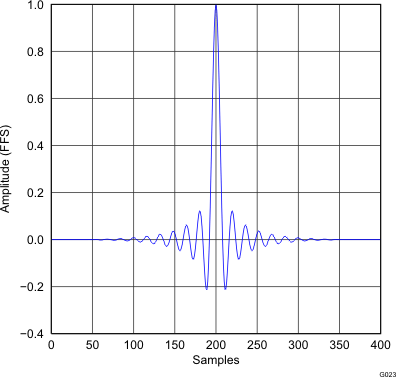 Figure 25. Normal x8 Interpolation Filter Impulse Response
Table 10. Normal x4 Interpolation Filter, Dual Rate
| Parameter | Condition | Value (Typical) | Value (Max) | Units |
| Filter Gain Pass Band | 0 ……. 0.45fS | ±0.01 | dB | |
| Filter Gain Stop Band | 0.55fS ….. 3.455fS | –60 | dB | |
| Filter Group Delay | 20tS | S |
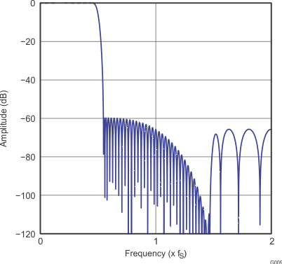 Figure 27. Normal x4 Interpolation Filter Frequency Response
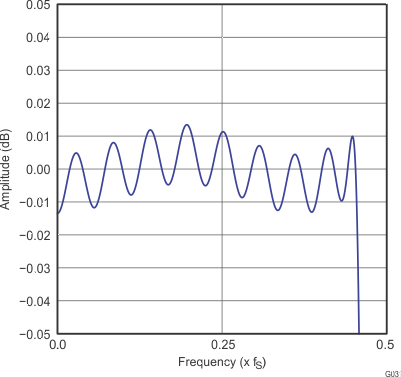 Figure 29. Normal x4 Interpolation Filter Passband Ripple
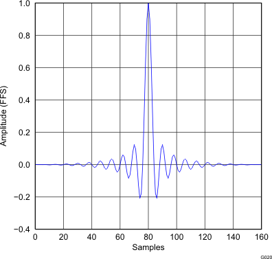 Figure 28. Normal x4 Interpolation Filter Impulse Response
Table 11. Normal x2 Interpolation Filter, Quad Rate
| Parameter | Condition | Value (Typical) | Value (Max) | Units |
| Filter Gain Pass Band | 0 ……. 0.45fS | ±0.01 | dB | |
| Filter Gain Stop Band | 0.55fS ….. 1.455fS | –60 | dB | |
| Filter Group Delay | 20tS | S |
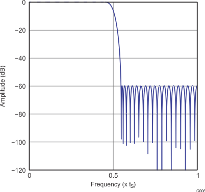 Figure 30. Normal x2 Interpolation Filter Frequency Response
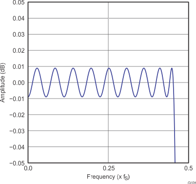 Figure 32. Normal x2 Interpolation Filter Passband Ripple
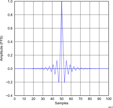 Figure 31. Normal x2 Interpolation Filter Impulse Response
Table 12. Low latency x8 Interpolation Filter, Single Rate
| Parameter | Condition | Value (Typical) | Value (Max) | Units |
| Filter Gain Pass Band | 0 ……. 0.45fS | ±0.001 | dB | |
| Filter Gain Stop Band | 0.55fS ….. 7.455fS | –52 | dB | |
| Filter Group Delay | 3.5tS | S |
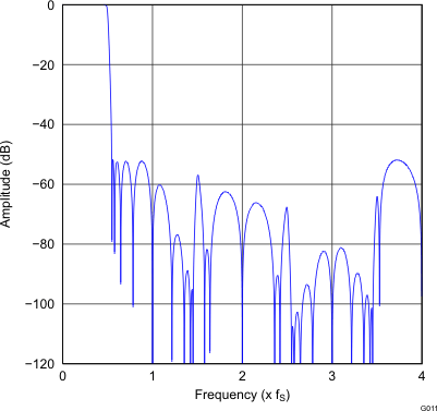 Figure 33. Low latency x8 Interpolation Filter Frequency Response
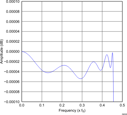 Figure 35. Low latency x8 Interpolation Filter Passband Ripple
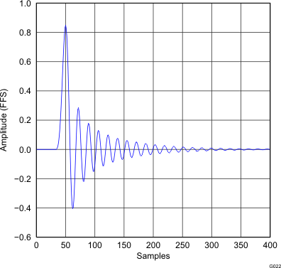 Figure 34. Low latency x8 Interpolation Filter Impulse Response
Table 13. Low latency x4 Interpolation Filter, Dual Rate
| Parameter | Condition | Value (Typical) | Value (Max) | Units |
| Filter Gain Pass Band | 0 ……. 0.45fS | ±0.001 | dB | |
| Filter Gain Stop Band | 0.55fS ….. 3.455fS | –52 | dB | |
| Filter Group Delay | 3.5tS | S |
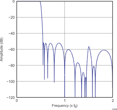 Figure 36. Low latency x4 Interpolation Filter Frequency Response
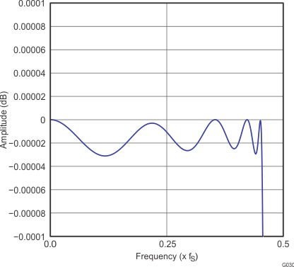 Figure 38. Low latency x4 Interpolation Filter Passband Ripple
 Figure 37. Low latency x4 Interpolation Filter Impulse Response
Table 14. Low latency ×2 Interpolation Filter, Quad Rate
| Parameter | Condition | Value (Typical) | Value (Max) | Units |
| Filter Gain Pass Band | 0 ……. 0.45fS | ±0.001 | dB | |
| Filter Gain Stop Band | 0.55fS ….. 1.455fS | –52 | dB | |
| Filter Group Delay | 3.5tS | S |
 Figure 39. Low latency x2 Interpolation Filter Frequency Response
Figure 41. Low latency x2 Interpolation Filter Passband Ripple
Figure 39. Low latency x2 Interpolation Filter Frequency Response
Figure 41. Low latency x2 Interpolation Filter Passband Ripple
 Figure 40. Low latency x2 Interpolation Filter Impulse Response
Table 15. Asymmetric FIR x8 Interpolation Filter, Single Rate
| Parameter | Condition | Value (Typical) | Value (Max) | Units |
| Filter Gain Pass Band | 0 ……. 0.40fS | ±0.05 | dB | |
| Filter Gain Stop Band | 0.72fS ….. 7.28fS | –50 | dB | |
| Filter Group Delay | 1.2tS | S |
 Figure 42. Asymmetric FIR x8 Interpolation Filter Frequency Response, Single Rate
 Figure 44. Asymmetric FIR x8 Interpolation Filter Passband Ripple, Single Rate
 Figure 43. Asymmetric FIR x8 Interpolation Filter Impulse Response, Single Rate
Table 16. Asymmetric FIR x4 Interpolation Filter, Dual Rate
| Parameter | Condition | Value (Typical) | Value (Max) | Units |
| Filter Gain Pass Band | 0 ……. 0.40fS | ±0.05 | dB | |
| Filter Gain Stop Band | 0.72fS ….. 3.28fS | –50 | dB | |
| Filter Group Delay | 1.2tS | S |
 Figure 45. Asymmetric FIR x4 Interpolation Filter Frequency Response, Dual Rate
 Figure 47. Asymmetric x4 Interpolation Filter Passband Ripple, Dual Rate
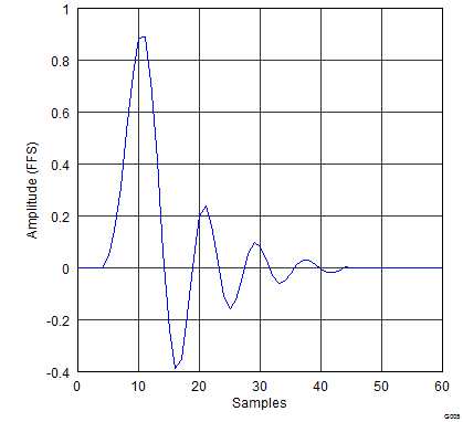 Figure 46. Asymmetric FIR x4 Interpolation Filter Impulse Response, Dual Rate
Table 17. Asymmetric FIR x2 Interpolation Filter, Quad Rate
| Parameter | Condition | Value (Typical) | Value (Max) | Units |
| Filter Gain Pass Band | 0 ……. 0.40fS | ±0.05 | dB | |
| Filter Gain Stop Band | 0.72fS ….. 1.28fS | –50 | dB | |
| Filter Group Delay | 1.2tS | S |
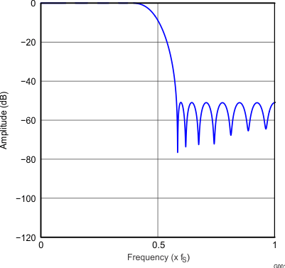 Figure 48. Asymmetric FIR x2 Interpolation Filter Frequency Response, Quad Rate
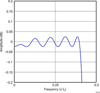 Figure 50. Asymmetric x2 Interpolation Filter Passband Ripple, Quad Rate
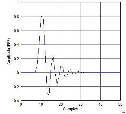 Figure 49. Asymmetric FIR x2 Interpolation Filter Impulse Response, Quad Rate
Table 18. High-Attentuation x8 Interpolation Filter, Single Rate
| Parameter | Condition | Value (Typical) | Value (Max) | Units |
| Filter Gain Pass Band | 0 ……. 0.45fS | ±0.0005 | dB | |
| Filter Gain Stop Band | 0.55fS ….. 7.455fS | –100 | dB | |
| Filter Group Delay | 33.7tS | S |
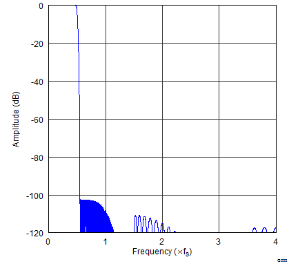 Figure 51. High-Attentuation x8 Interpolation Filter Frequency Response, Single Rate
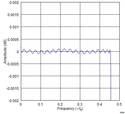 Figure 53. High-Attentuation x8 Interpolation Filter Passband Ripple, Single Rate
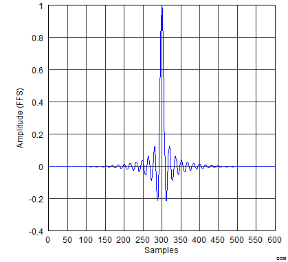 Figure 52. High-Attentuation x8 Interpolation Filter Impulse Response, Single Rate
Table 19. High-Attentuation x4 Interpolation Filter, Dual Rate
| Parameter | Condition | Value (Typical) | Value (Max) | Units |
| Filter Gain Pass Band | 0 ……. 0.45fS | ±0.0005 | dB | |
| Filter Gain Stop Band | 0.55fS ….. 3.455fS | –100 | dB | |
| Filter Group Delay | 33.7tS | S |
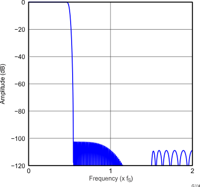 Figure 54. High-Attentuation x4 Interpolation Filter Frequency Response, Dual Rate
 Figure 56. High-Attentuation x4 Interpolation Filter Passband Ripple, Dual Rate
 Figure 55. High-Attentuation x4 Interpolation Filter Impulse Response, Dual Rate
Table 20. High-Attentuation x2 Interpolation Filter, Quad Rate
| Parameter | Condition | Value (Typical) | Value (Max) | Units |
| Filter Gain Pass Band | 0 ……. 0.45fS | ±0.0005 | dB | |
| Filter Gain Stop Band | 0.55fS ….. 1.455fS | –100 | dB | |
| Filter Group Delay | 33.7tS | S |
 Figure 57. High-Attentuation x2 Interpolation Filter Frequency Response, Quad Rate
 Figure 59. High-Attentuation x2 Interpolation Filter Passband Ripple, Quad Rate
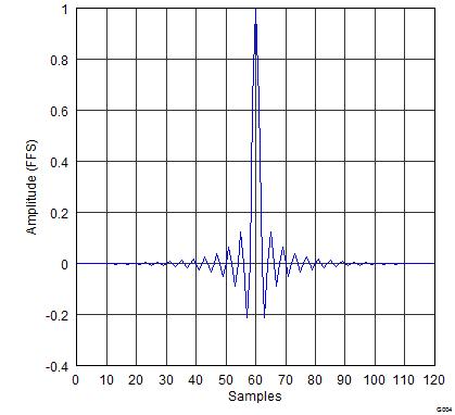 Figure 58. High-Attentuation x2 Interpolation Filter Impulse Response, Quad Rate
8.6.3 Fixed Audio Processing Flow (Program 5)
The PCM5242 implements signal processing capabilities and interpolation filtering via processing blocks. These fixed processing blocks give users the choice of how much and what type of signal processing they may use and which interpolation filter is applied.
The signal processing blocks available are:
- Biquad filters
- Multiband DRC
- Mono mixer
- Stereo mixer
- Master volume
The addresses of the coefficients are fixed when selecting the fixed processing flow, however, if these components are used in the RAM source mode (Program 31) the registers for coefficients will change. Users can find more details in Purepath Studio.
NOTE
This process flow requires 1024 instruction cycles. Therefore, it will only function at sampling frequencies up to 48kHz.
8.6.3.1 Processing Blocks – Detailed Descriptions
Figure 60 shows the fixed processing flow.
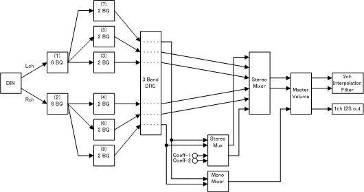 Figure 60. Preset Process Flow
Figure 61 shows a screen capture of PurePath Studio.
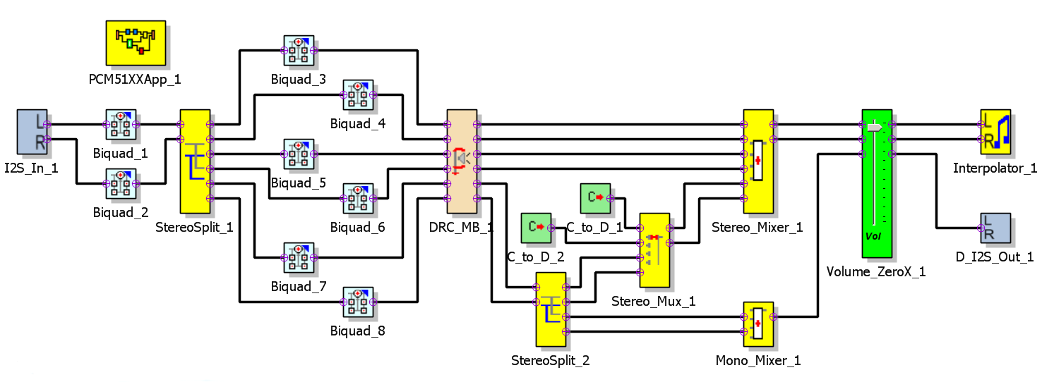 Figure 61. PurePath Studio Screen Capture
8.6.3.2 Biquad Section
The transfer function of each of the biquad filters is given by
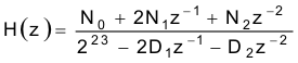
 Figure 62. Biquad Block
Table 21. Biquad Filter Coefficients
| Filter | Channel | Coefficient | Register |
|---|---|---|---|
| BIQUAD (1) - 1 BIQUAD (2) - 1 | Lch, Rch |
N0 | C10 (Pg 44, Reg 48,49,50,51) |
| N1 | C11 (Pg 44, Reg 52,53,54,55) | ||
| N2 | C12 (Pg 44, Reg 56,57,58,59) | ||
| D1 | C13 (Pg 44, Reg 60,61,62,63) | ||
| D2 | C14 (Pg 44, Reg 64,65,66,67) | ||
| BIQUAD (1) - 2 BIQUAD (2) - 2 | Lch, Rch |
N0 | C15 (Pg 44, Reg 68,69,70,71) |
| N1 | C16 (Pg 44, Reg 72,73,74,75) | ||
| N2 | C17 (Pg 44, Reg 76,77,78,79) | ||
| D1 | C18 (Pg 44, Reg 80,81,82,83) | ||
| D2 | C19 (Pg 44, Reg 84,85,86,87) | ||
| BIQUAD (1) - 3 BIQUAD (2) - 3 | Lch, Rch |
N0 | C20 (Pg 44, Reg 88,89,90,91) |
| N1 | C21 (Pg 44, Reg 92,93,94,95) | ||
| N2 | C22 (Pg 44, Reg 96,97,98,99) | ||
| D1 | C23 (Pg 44, Reg 100,101, 102, 103) | ||
| D2 | C24 (Pg 44, Reg 104, 105, 106, 107) | ||
| BIQUAD (1) - 4 BIQUAD (2) - 4 | Lch, Rch |
N0 | C25 (Pg 44, Reg 108, 109, 110, 111) |
| N1 | C26 (Pg 44, Reg 112, 113, 114, 115) | ||
| N2 | C27 (Pg 44, Reg 116, 117, 118, 119) | ||
| D1 | C28 (Pg 44, Reg 120, 121, 122, 123) | ||
| D2 | C29 (Pg 44, Reg 124, 125, 126, 127) | ||
| BIQUAD (1) - 5 BIQUAD (2) - 5 | Lch, Rch |
N0 | C30 (Pg 45, Reg 8, 9, 10, 11) |
| N1 | C31 (Pg 45, Reg 12, 13, 14, 15) | ||
| N2 | C32 (Pg 45, Reg 16, 17, 18, 19) | ||
| D1 | C33 (Pg 45, Reg 20, 21, 22, 23) | ||
| D2 | C34 (Pg 45, Reg 24, 25, 26, 27) | ||
| BIQUAD (1) - 6 BIQUAD (2) - 6 | Lch, Rch |
N0 | C35 (Pg 45, Reg 28, 29, 30, 31) |
| N1 | C36 (Pg 45, Reg 32, 33, 34, 35) | ||
| N2 | C37 (Pg 45, Reg 36, 37, 38, 39) | ||
| D1 | C38 (Pg 45, Reg 40, 41, 42, 43) | ||
| D2 | C39 (Pg 45, Reg 44, 45, 46, 47) | ||
| BIQUAD (3) - 1 BIQUAD (4) - 1 | Lch, Rch |
N0 | C40 (Pg 45, Reg 48, 49, 50, 51) |
| N1 | C41 (Pg 45, Reg 52, 53, 54, 55) | ||
| N2 | C42 (Pg 45, Reg 56, 57, 58, 59) | ||
| D1 | C43 (Pg 45, Reg 60, 61, 62, 63) | ||
| D2 | C44 (Pg 45, Reg 64, 65, 66, 67) | ||
| BIQUAD (3) - 2 BIQUAD (4) - 2 | Lch, Rch |
N0 | C45 (Pg 45, Reg 68, 69, 70, 71) |
| N1 | C46 (Pg 45, Reg 72, 73, 74, 75) | ||
| N2 | C47 (Pg 45, Reg 76, 77, 78, 79) | ||
| D1 | C48 (Pg 45, Reg 80, 81, 82, 83) | ||
| D2 | C49 (Pg 45, Reg 84, 85, 86, 87) | ||
| BIQUAD (5) - 1 BIQUAD (6) - 1 | Lch, Rch |
N0 | C50 (Pg 45, Reg 88, 89, 90, 91) |
| N1 | C51 (Pg 45, Reg 92, 93, 94, 95) | ||
| N2 | C52 (Pg 45, Reg 96, 97, 98, 99) | ||
| D1 | C53 (Pg 45, Reg 100, 101, 102, 103) | ||
| D2 | C54 (Pg 45, Reg 104, 105, 106, 107) | ||
| BIQUAD (5) - 2 BIQUAD (6) - 2 | Lch, Rch |
N0 | C55 (Pg 45, Reg 108, 109, 110, 111) |
| N1 | C56 (Pg 45, Reg 112, 113, 114, 115) | ||
| N2 | C57 (Pg 45, Reg 116, 117, 118, 119) | ||
| D1 | C58 (Pg 45, Reg 120, 121, 122, 123) | ||
| D2 | C59 (Pg 45, Reg 124, 125, 126, 127) | ||
| BIQUAD (7) - 1 BIQUAD (8) - 1 | Lch, Rch |
N0 | C60 (Pg 46, Reg 8, 9, 10, 11) |
| N1 | C61 (Pg 46, Reg 12, 13, 14, 15) | ||
| N2 | C62 (Pg 46, Reg 16, 17, 18, 19) | ||
| D1 | C63 (Pg 46, Reg 20, 21, 22, 23) | ||
| D2 | C64 (Pg 46, Reg 24, 25, 26, 27) | ||
| BIQUAD (7) - 2 BIQUAD (8) - 2 | Lch, Rch |
N0 | C65 (Pg 46, Reg 28, 29, 30, 31) |
| N1 | C66 (Pg 46, Reg 32, 33, 34, 35) | ||
| N2 | C67 (Pg 46, Reg 36, 37, 38, 39) | ||
| D1 | C68 (Pg 46, Reg 40, 41, 42, 43) | ||
| D2 | C69 (Pg 46, Reg 44, 45, 46, 47) |
8.6.3.3 Dynamic Range Compression
Dynamic range compression (DRC) improves the overall listening experience. Typical music signals are characterized by crest factors (the ratio of peak signal power to average signal power) of 12dB or more. To avoid audible distortion due to clipping of peak signals, the gain of the DAC channel must be adjusted so as not to cause hard clipping. As a result, the low applied gain during nominal periods causes the perception that the signal is not loud enough. To overcome this problem, the DRC in the PCM5242 continuously monitors the output of the DAC Digital Volume control to detect its power level with respect to 0dB full-scale. When the power level is low, the DRC increases the input signal gain to make it sound louder, and reduces the gain during peaks to avoid hard clipping. The DRC enables louder audio during nominal periods with a clearer, more pleasant listening experience.
The 3-band DRC function applies DRC to 3 different mono/stereo signals with 3 different time constants. The same DRC curve is applied on all the signals, enabling a multi-band DRC solution. The underlying DRC algorithm is the same as that available with the DRC component in PurePath Studio. In this instance, the DRC gain acts on each signal in time-multiplexed order, for example, 1-2-3, 1-2-3, 1-2-3.
Table 22. DRC Coefficients
| Coefficient | Register | Description |
|---|---|---|
| DRC_MB_1_DRC_1_DRCAE | C70 (Pg 46, Reg 48, 49, 50, 51) | |
| DRC_MB_1_DRC_1_DRC1AE | C71 (Pg 46, Reg 52, 53, 54, 55) | |
| DRC_MB_1_DRC_1_DRCAA | C72 (Pg 46, Reg 56, 57, 58, 59) | |
| DRC_MB_1_DRC_1_DRC1AA | C73 (Pg 46, Reg 60, 61, 62, 63) | |
| DRC_MB_1_DRC_1_DRCAD | C74 (Pg 46, Reg 64, 65, 66, 67) | |
| DRC_MB_1_DRC_1_DRC1AD | C75 (Pg 46, Reg 68, 69, 70, 71) | |
| DRC_MB_1_DRC_2_DRCAE | C76 (Pg 46, Reg 72, 73, 74, 75) | |
| DRC_MB_1_DRC_2_DRC1AE | C77 (Pg 46, Reg 76, 77, 78, 79) | |
| DRC_MB_1_DRC_2_DRCAA | C78 (Pg 46, Reg 80, 81, 82, 83) | |
| DRC_MB_1_DRC_2_DRC1AA | C79 (Pg 46, Reg 84, 85, 86, 87) | |
| DRC_MB_1_DRC_2_DRCAD | C80 (Pg 46, Reg 88, 89, 90, 91) | |
| DRC_MB_1_DRC_2_DRC1AD | C81 (Pg 46, Reg 92, 93, 94, 95) | |
| DRC_MB_1_DRC_3_DRCAE | C82 (Pg 46, Reg 96, 97, 98, 99) | |
| DRC_MB_1_DRC_3_DRC1AE | C83 (Pg 46, Reg 100, 101, 102, 103) | |
| DRC_MB_1_DRC_3_DRCAA | C84 (Pg 46, Reg 104, 105, 106, 107) | |
| DRC_MB_1_DRC_3_DRC1AA | C85 (Pg 46, Reg 108, 109, 119, 111) | |
| DRC_MB_1_DRC_3_DRCAD | C86 (Pg 46, Reg 112, 113, 114, 115) | |
| DRC_MB_1_DRC_3_DRC1AD | C87 (Pg 46, Reg 116, 117, 118, 119) | |
| DRC_MB_1_DRC_DRCK0 | C88 (Pg 46, Reg 120, 121, 122, 123) | |
| DRC_MB_1_DRC_DRCK1 | C89 (Pg 46, Reg 124, 125, 126, 127) | |
| DRC_MB_1_DRC_DRCK2 | C90 (Pg 47, Reg 8, 9, 10, 11) | |
| DRC_MB_1_DRC_DRCMT1 | C91 (Pg 47, Reg 12, 13, 14, 15) | |
| DRC_MB_1_DRC_DRCMT2 | C92 (Pg 47, Reg 16, 17, 18, 19) | |
| DRC_MB_1_DRC_DRCOFF1 | C93 (Pg 47, Reg 20, 21, 22, 23) | |
| DRC_MB_1_DRC_DRCOFF2 | C94 (Pg 47, Reg 24, 25, 26, 27) | |
| DRC_MB_1_MinusOne_Q22 | C95 (Pg 47, Reg 28, 29, 30, 31) | |
| DRC_MB_1_MinusTwo_Q22 | C96 (Pg 47, Reg 32, 33, 34, 35) | |
| DRC_MB_1_One_M2 | C97 (Pg 47, Reg 36, 37, 38, 39) | |
| DRC_MB_1_Zero | C98 (Pg 47, Reg 40, 41, 42, 43) | |
| DRC_MB_1_En_dB | C99 (Pg 47, Reg 44, 45, 46, 47) | |
| DRC_MB_1_Minus__Zero_dB | C100 (Pg 47, Reg 48, 49, 50, 51) | |
| DRC_MB_1_60_dB | C101 (Pg 47, Reg 52, 53, 54, 55) | |
| DRC_MB_1_Minus_60_dB | C102 (Pg 47, Reg 56, 57, 58, 59) | |
| DRC_MB_1_12_dB | C103 (Pg 47, Reg 60, 61, 62, 63) | |
| DRC_MB_1_Offset | C104 (Pg 47, Reg 64, 65, 66, 67) | |
| DRC_MB_1_K | C105 (Pg 47, Reg 68, 69, 70, 71) | |
| DRC_MB_1_x / DRC_MB_1_DRC | C106 (Pg 47, Reg 72, 73, 74, 75) | |
| DRC_MB_1_48_dB | C107 (Pg 47, Reg 76, 77, 78, 79) | |
| DRC_MB_1_Minus_48_dB | C108 (Pg 47, Reg 80, 81, 82, 83) | |
| DRC_MB_1_c1_3 | C109 (Pg 47, Reg 84, 85, 86, 87) | |
| DRC_MB_1_c1_2 | C110 (Pg 47, Reg 88, 89, 90, 91) | |
| DRC_MB_1_c1_1 | C111 (Pg 47, Reg 92, 93, 94, 95) | |
| DRC_MB_1_c1_0 | C112 (Pg 47, Reg 96, 97, 98, 99) | |
| DRC_MB_1_O1_1 | C113 (Pg 47, Reg 100, 101, 102, 103) | |
| DRC_MB_1_S1_1 | C114 (Pg 47, Reg 104, 105, 106, 107) | |
| DRC_MB_1_O1_2 | C115 (Pg 47, Reg 108, 109, 119, 111) | |
| DRC_MB_1_S1_2 | C116 (Pg 47, Reg 112, 113, 114, 115) | |
| DRC_MB_1_O1_3 | C117 (Pg 47, Reg 116, 117, 118, 119) | |
| DRC_MB_1_S1_3 | C118 (Pg 47, Reg 120, 121, 122, 123) | |
| DRC_MB_1_One_1_Q17 | C119 (Pg 47, Reg 124, 125, 126, 127) | |
| DRC_MB_1_Scale1 | C120 (Pg 48, Reg 8, 9, 10, 11) | |
| DRC_MB_1_x1Coeff | C121 (Pg 48, Reg 12, 13, 14, 15) | |
| DRC_MB_1_c2_3 | C122 (Pg 48, Reg 16, 17, 18, 19) | |
| DRC_MB_1_c2_2 | C123 (Pg 48, Reg 20, 21, 22, 23) | |
| DRC_MB_1_c2_1 | C124 (Pg 48, Reg 24, 25, 26, 27) | |
| DRC_MB_1_c2_0 | C125 (Pg 48, Reg 28, 29, 30, 31) | |
| DRC_MB_1_O2_1 | C126 (Pg 48, Reg 32, 33, 34, 35) | |
| DRC_MB_1_S2_1 | C127 (Pg 48, Reg 36, 37, 38, 39) | |
| DRC_MB_1_O2_2 | C128 (Pg 48, Reg 40, 41, 42, 43) | |
| DRC_MB_1_S2_2 | C129 (Pg 48, Reg 44, 45, 46, 47) | |
| DRC_MB_1_O2_3 | C130 (Pg 48, Reg 48, 49, 50, 51) | |
| DRC_MB_1_S2_3 | C131 (Pg 48, Reg 52, 53, 54, 55) | |
| DRC_MB_1_One_2_Q17 | C132 (Pg 48, Reg 56, 57, 58, 59) | |
| DRC_MB_1_Scale2 | C133 (Pg 48, Reg 60, 61, 62, 63) | |
| DRC_MB_1_x2Coeff | C134 (Pg 48, Reg 64, 65, 66, 67) | |
| DRC_MB_1_R1_1 | C135 (Pg 48, Reg 68, 69, 70, 71) | |
| DRC_MB_1_R1_2 | C136 (Pg 48, Reg 72, 73, 74, 75) | |
| DRC_MB_1_R2_1 | C137 (Pg 48, Reg 76, 77, 78, 79) | |
| DRC_MB_1_R2_2 | C138 (Pg 48, Reg 80, 81, 82, 83) | |
| DRC_MB_1_Band1_GainC | C139 (Pg 48, Reg 84, 85, 86, 87) | |
| DRC_MB_1_Band2_GainC | C140 (Pg 48, Reg 88, 89, 90, 91) | |
| DRC_MB_1_Band3_GainC | C141 (Pg 48, Reg 92, 93, 94, 95) | |
| DRC_MB_1_MinusOne_M1 | C142 (Pg 48, Reg 96, 97, 98, 99) | |
| DRC_MB_1_One_M1 | C143 (Pg 48, Reg 100, 101, 102, 103) | |
| DRC_MB_1_Band1_GainE | C144 (Pg 48, Reg 104, 105, 106, 107) | |
| DRC_MB_1_Band2_GainE | C145 (Pg 48, Reg 108, 109, 110, 111) | |
| DRC_MB_1_Band3_GainE | C146 (Pg 48, Reg 112, 113, 114, 115) | |
| DRC_MB_1_minus_One_M2 | C147 (Pg 48, Reg 116, 117, 118, 119) |
8.6.3.4 Stereo Mixer
Three stereo inputs are mixed into one stereo output with input signal gain given by Equation 2.

where
- i=1:2,3
Figure 63 and Table 23 show the strereo mixer operation.
 Figure 63. Stereo Mixer Block
Table 23. Stereo Mixer Coefficients
| Coefficient | Register | Description |
|---|---|---|
| Stereo_Mixer_1_MixGain1 | C148 (Pg 48, Reg 120, 121, 122, 123) | |
| Stereo_Mixer_1_MixGain2 | C149 (Pg 48, Reg 124, 125, 126, 127) | |
| Stereo_Mixer_1_MixGain3 | C150 (Pg 49, Reg 8, 9, 10, 11) |
8.6.3.5 Stereo Multiplexer
The Stereo Multiplexer selects one or 2 from 4 stereo input channels.
 Figure 64. Stereo Multiplexer Block
Table 24. Stereo Multiplexer Select Coefficient
| Coefficient | Register | Description |
|---|---|---|
| Stereo_Mux_1_MuxSelect | C152 (Pg 49, Reg 16, 17, 18, 19) |
Table 25. Stereo Multiplexer Input Coefficient
| Coefficient | Register | Description |
|---|---|---|
| C_to_D_1_Coefval C_to_D_2_Coefval |
C153 (Pg 49, Reg 20, 21, 22, 23) |
8.6.3.6 Mono Mixer
The Mono Mixer computes a weighted sum of 2 input channels and produces an output.
 Figure 65. Mono Mixer Block
Table 26. Mono Mixer Coefficients
| Coefficient | Register | Description |
|---|---|---|
| Mono_Mixer_1_MixGain1 | C154 (Pg 49, Reg 24, 25, 26, 27) | |
| Mono_Mixer_1_MixGain2 | C155 (Pg 49, Reg 28, 29, 30, 31) |
8.6.3.7 Master Volume Control
The Master Volume controls the volume using a linear ramp and zero crossing detection for transitions.
Table 27. Mono Mixer Coefficients
| Coefficient | Register | Description |
|---|---|---|
| Volume_ZeroX_1_volcmd | C158 (Pg 49, Reg 40, 41, 42, 43) | |
| Volume_ZeroX_1_volout | C159 (Pg 49, Reg 44, 45, 46, 47) | |
| Volume_ZeroX_1_volout_loudness | C160 (Pg 49, Reg 48, 49, 50, 51) | |
| Volume_ZeroX_1_MinusOne_M2 | C161 (Pg 49, Reg 52, 53, 54, 55) | |
| Volume_ZeroX_1_workingval_1_pre_CRAM | C162 (Pg 49, Reg 56, 57, 58, 59) | |
| Volume_ZeroX_1_volout_pre1 | C163 (Pg 49, Reg 60, 61, 62, 63) | |
| Volume_ZeroX_1_workingval_2_pre_CRAM | C164 (Pg 49, Reg 64, 65, 66, 67) | |
| Volume_ZeroX_1_volout_pre2 | C165 (Pg 49, Reg 68, 69, 70, 71) | |
| Volume_ZeroX_1_workingval_3_pre_CRAM | C166 (Pg 49, Reg 72, 73, 74, 75) | |
| Volume_ZeroX_1_volout_pre3 | C167 (Pg 49, Reg 76, 77, 78, 79) | |
| Volume_ZeroX_1_One_M2 | C168 (Pg 49, Reg 80, 81, 82, 83) | |
| Volume_ZeroX_1_Zero | C169 (Pg 49, Reg 84, 85, 86, 87) | |
| MinusOne_Int | C170 (Pg 49, Reg 88, 89, 90, 91) | |
| MinusOne_M1 | C171 (Pg 49, Reg 92, 93, 94, 95) | |
| One_M2 | C172 (Pg 49, Reg 96, 97, 98, 99) | |
| One_M1 | C173 (Pg 49, Reg 100, 101, 102, 103) | |
| Zero | C174 (Pg 49, Reg 104, 105, 106, 107) |
8.6.3.8 Miscellaneous Coefficients
Table 28. Miscellaneous Coefficients
| Coefficient | Register | Description |
|---|---|---|
| DRC_MB_1_DataBlock | C175 (Pg 49, Reg 108, 109, 110, 111) | |
| DRC_MB_1_CoeffBlock | C176 (Pg 49, Reg 112, 113, 114, 115) | |
| Volume_ZeroX_1_DataBlock | C177 (Pg 49, Reg 116, 117, 118, 119) | |
| Volume_ZeroX_1_CoeffBlock | C178 (Pg 49, Reg 120, 121, 122, 123) | |
| plus_one | C179 (Pg 49, Reg 124, 125, 126, 127) | |
| ADD_OF_filter_in_L | C180 (Pg 50, Reg 8, 9, 10, 11) | |
| ADD_OF_filter_in_R | C181 (Pg 50, Reg 12, 13, 14, 15) |
8.7 DAC and Differential Analog Outputs
8.7.1 Analog Outputs
The PCM5242 devices include a two-channel DAC, with differential outputs. Each pin has a full-scale output voltage is 2.1Vrms with ground center output. This equates to a 4.2Vrms differential output. A dc-coupled load is supported in addition to an ac-coupled load, if the load resistance conforms to the specification. The PCM5242 DAC outputs on the OUTLP, OUTLN, OUTRP, and OUTRN terminals have market-leading low out-of-band noise, which offer up to 20dB lower out-of-band noise compared with existing DAC technology.
Many applications require an external low-pass RC filter (470Ω + 1.2nF) to provide sufficient out-of-band noise rejection. This RC filter provides the added advantage of improved protection against ESD damage.
The PCM5242 can also support single ended outputs, using OUTLP and OUTRP respectively. A single 470Ω and 2.2nF capacitor can be used on each pin in single ended mode.
The choice between VREF and VCOM modes affects the maximum output level. This is explained in Voltage Reference and Output Levels.
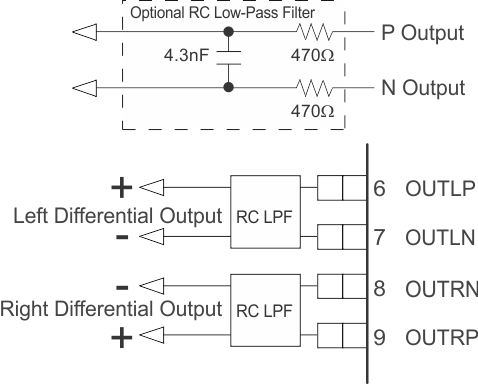 Figure 66. Optional Low Pass Filters
8.7.2 Choosing Between VREF and VCOM Modes
VREF mode is the default configuration. This mode allows full 2.1Vrms signal output. As shown in Recommended Operating Conditions, the minimum AVDD to avoid clipping is 3.2V.
VCOM mode allows setting a custom common-mode voltage when required by the application. This somewhat limits the output signal swing before clipping.
8.7.2.1 Voltage Reference and Output Levels
The PCM5242 has an internal, fixed band-gap reference voltage, with default operation in VREF mode. No external decoupling capacitor is required for this mode.
The PCM5242 can be operated with a common-mode voltage output (VCOM mode) at the VCOM pin by setting Page 1, Register 1, D(0) to 1. In this mode, an external decoupling capacitor is required.
When using this DAC in VREF mode, the output-signal voltage is independent of the power-supply voltage: The D/A conversion gain in VREF mode yields a 2.1Vrms output voltage with a digital full-scale input. However, in VREF mode, an output waveform may clip due to the limitations that may be present in the analog power supply voltage. On the other hand, the full-scale output voltage in VCOM mode is proportional to the analog power supply AVDD. Example, (2.1 × AVDD / 3.3) Vrms.
8.7.2.2 Mode Switching Sequence, From VREF Mode to VCOM Mode
Following register setting sequence is recommended for changing VREF mode to VCOM mode.
| 1. | Page 0 / Register 2 | RQST = 1: Standby mode |
| 2. | Page 1 / Register 8 | RCMF = 1: Fast ramp up → on |
| 3. | Page 1 / Register 9 | VCPD = 0: VCOM is power on |
| 4. | Wait 3ms with external capacitor = 1µF | |
| 5. | Page 1 / Register 8 | RCMF = 0: Fast ramp up → off |
| 6. | Page 1 / Register 1 | OSEL = 1: VCOM mode |
| 7. | Page 0 / Register 2 | RQST = 0: Normal mode |
8.7.3 Digital Volume Control
A basic digital volume control with range from 24 dB to -103 dB and mute is available on each channels by Page 0, Resister 61, D(7:0) for L-ch and Register 62, D(7:0) for R-ch. These volume controls all have 0.5 dB step programmability over most gain and attenuation ranges. Table 29 lists the detailed gain versus programmed setting for this basic volume control. Volume can be changed for both L-ch and R-ch at the same time or independently by Page 0, Register 60, D(1:0). When D(1:0) set 00 (default), independent control is selected. When D(1:0) set 01, R-ch accords with L-ch volume. When D(1:0) set 10, L-ch accords with R-ch volume. To set D(1:0) to 11 is prohibited.
NOTE
This volume control is done externally to the miniDSP and only influences the analog DAC output. Any changes to the SDOUT data should be done in the miniDSP process flow
Table 29. Digital Volume Control Settings
| Gain Setting | Binary Data | Gain (dB) | Comments |
| 0 | 0000-0000 | 24.0 | Positive maximum |
| 1 | 0000-0001 | 23.5 | |
| : | : | : | |
| 46 | 0010-1110 | 1.0 | |
| 47 | 0010-1111 | 0.5 | |
| 48 | 0011-0000 | 0.0 | No attenuation (default) |
| 49 | 0011-0001 | - 0.5 | |
| 50 | 0011-0010 | - 1.0 | |
| 51 | 0011-0011 | - 1.5 | |
| : | : | : | |
| 253 | 1111-1101 | - 102.5 | |
| 254 | 1111-1110 | - 103 | Negative maximum |
| 255 | 1111-1111 | - ∞ | Negative infinite (Mute) |
Ramp-up frequency and ramp-down frequency can be controlled by Page 0, Register 63, D(7:6) and D(3:2) as shown in Table 30. Also Ramp-up step and ramp-down step can be controlled by Page 0, Register 63 D(5:4) and D(1:0) as shown in Table 31.
Table 30. Ramp Up or Down Frequency
| Ramp up speed | Every N fS | Comments | Ramp down frequency | Every N fS | Comments |
| 00 | 1 | Default | 00 | 1 | Default |
| 01 | 2 | 01 | 2 | ||
| 10 | 4 | 10 | 4 | ||
| 11 | Direct change | 11 | Direct change |
Table 31. Ramp Up or Down Step
| Ramp up step | Step dB | Comments | Ramp down step | Step dB | Comments |
| 00 | 4.0 | 00 | -4.0 | ||
| 01 | 2.0 | 01 | -2.0 | ||
| 10 | 1.0 | Default | 10 | -1.0 | Default |
| 11 | 0.5 | 11 | -0.5 |
8.7.3.1 Emergency Ramp Down
Digital volume emergency ramp down by is provided for situations such as I2S clock error and power supply failure. Ramp-down speed is controlled by Page 0, Register 64, D(7:6). Ramp-down step can be controlled by Page 0 Register 64, D(5:4). Default is ramp-down by every fS cycle with -4dB step.
8.7.4 Analog Gain Control
Analog gain control can be selected between 2Vrms FS (0dB) or 1Vrms FS (-6dB). Gain is controlled via hardware by the AGNS pin, and via software (SPI/I2C), Page 1, Register 2, D4(L-ch) / D0(R-ch).
8.8 Reset and System Clock Functions
8.8.1 Clocking Overview
The PCM5242 devices have flexible systems for clocking. Internally, the device requires a number of clocks, mostly at related clock rates to function correctly. All of these clocks can be derived from the Serial Audio Interface in one form or another.
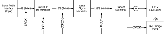 Figure 67. Audio flow with respective clocks
As shown in Figure 67 the basic data flow at basic sample rate (fS). Once the data is brought into the serial audio interface, it gets processed, interpolated and modulated all the way to 128 × fS before arriving at the current segments for the final digital to analog conversion.
The clock tree is shown in Figure 68.
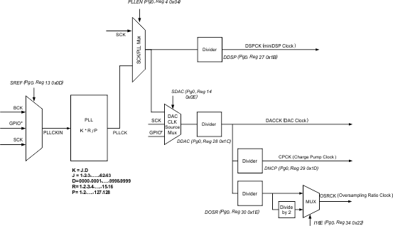 Figure 68. PCM5242 Clock Distribution Tree
The Serial Audio Interface typically has 4 connections SCK (System Master Clock), BCK (Bit Clock), LRCK (Left Right Word Clock) and Data. The device has an internal PLL that is used to take either SCK or BCK and create the higher rate clocks required by the miniDSP and the DAC clock.
In situations where the highest audio performance is required, it’s suggested that the SCK is brought to the device, along with BCK and LRCK. The device should be configured so that the PLL is only providing a clock source to the miniDSP. By ensuring that the DACCK (DAC Clock) is being driven by the external SCK source, jitter evident in the PLL (in all PLL's) is kept out of the DAC, Charge Pump and Oversampling system.
Everything else should be a division of the incoming SCK. This is done by setting DAC CLK Source Mux (SDAC in the diagram above) to use SCK as a source, rather than the output of the SCK/PLL Mux. Code Examples for this are available in SLAC622
When the Auto Clock Configuration bit is set (Page0/ Register 0x25), no additional clocks configuration is required. However, when setting custom PLL values etc, the target output rates should match those shown in the recommended PLL values of Table 50.
8.8.2 Clock Slave Mode With Master Clock (SCK) Input (4 Wire I2S)
The PCM5242 requires a system clock to operate the digital interpolation filters and advanced segment DAC modulators. The system clock is applied at the SCK input and supports up to 50MHz. The PCM5242 system-clock detection circuit automatically senses the system-clock frequency. Common audio sampling frequencies in the bands of 8kHz, 16kHz, (32kHz - 44.1kHz - 48kHz), (88.2kHz - 96kHz), (176.4kHz -192kHz), and 384kHz with ±4% tolerance are supported. Values in the parenthises are "grouped" when detected, e.g. 88.2kHZ and 96kHz are detected as "double rate", 32kHz, 44.1kHz and 48kHz will be detected as "single rate".
In the presence of a valid bit SCK, BCK and LRCK in software mode, the device will autoconfigure the clock tree and PLL to drive the miniDSP as required.
The sampling frequency detector sets the clock for the digital filter, Delta Sigma Modulator (DSM) and the Negative Charge Pump (NCP) automatically. Table 32 shows examples of system clock frequencies for common audio sampling rates.
SCK rates that are not common to standard audio clocks, between 1MHz and 50MHz, are only supported in software mode by configuring various PLL and clock-divider registers. This programmability allows the device to become a clock master and drive the host serial port with LRCK and BCK, from a non-audio related clock (for example, using 12MHz to generate 44.1kHz (LRCK) and 2.8224MHz (BCK) ).
Table 32. System Master Clock Inputs for Audio Related Clocks
| Sampling Frequency | System Clock Frequency (fSCK) (MHz) | |||||||||||
| 64 fS | 128 fS | 192 fS | 256 fS | 384 fS | 512 fS | 768 fS | 1024 fS | 1152 fS | 1536 fS | 2048 fS | 3072 fS | |
| 8 kHz | –(1) | 1.0240(2) | 1.5360(2) | 2.0480 | 3.0720 | 4.0960 | 6.1440 | 8.1920 | 9.2160 | 12.2880 | 16.3840 | 24.5760 |
| 16 kHz | –(1) | 2.0480(2) | 3.0720(2) | 4.0960 | 6.1440 | 8.1920 | 12.2880 | 16.3840 | 18.4320 | 24.5760 | 36.8640 | 49.1520 |
| 32 kHz | –(1) | 4.0960(2) | 6.1440(2) | 8.1920 | 12.2880 | 16.3840 | 24.5760 | 32.7680 | 36.8640 | 49.1520 | –(1) | –(1) |
| 44.1 kHz | –(1) | 5.6488(2) | 8.4672(2) | 11.2896 | 16.9344 | 22.5792 | 33.8688 | 45.1584 | –(1) | –(1) | –(1) | –(1) |
| 48 kHz | –(1) | 6.1440(2) | 9.2160(2) | 12.2880 | 18.4320 | 24.5760 | 36.8640 | 49.1520 | –(1) | –(1) | –(1) | –(1) |
| 88.2 kHz | –(1) | 11.2896(2) | 16.9344 | 22.5792 | 33.8688 | 45.1584 | –(1) | –(1) | –(1) | –(1) | –(1) | –(1) |
| 96 kHz | –(1) | 12.2880(2) | 18.4320 | 24.5760 | 36.8640 | 49.1520 | –(1) | –(1) | –(1) | –(1) | –(1) | –(1) |
| 176.4 kHz | –(1) | 22.5792 | 33.8688 | 45.1584 | –(1) | –(1) | –(1) | –(1) | –(1) | –(1) | –(1) | –(1) |
| 192 kHz | –(1) | 24.5760 | 36.8640 | 49.1520 | –(1) | –(1) | –(1) | –(1) | –(1) | –(1) | –(1) | –(1) |
| 384 kHz | 24.5760 | 49.1520 | –(1) | –(1) | –(1) | –(1) | –(1) | –(1) | –(1) | –(1) | –(1) | –(1) |
See Timing Requirements: PCM Audio Data for clock timing requirements.
8.8.3 Clock Slave Mode with BCK PLL to Generate Internal Clocks (3-Wire PCM)
The system clock PLL mode allows designers to use a simple 3-wire I2S audio source. The 3-wire source reduces the need for a high frequency SCK, making PCB layout easier, and reduces high frequency electromagnetic interference.
In hardwired mode, the internal PLL is disabled as soon as an external SCK is supplied.
In hardwired mode, the device starts up expecting an external SCK input, but if BCK and LRCK start correctly while SCK remains at ground level for 16 successive LRCK periods, then the internal PLL starts, automatically generating an internal SCK from the BCK reference. Specific BCK rates are required to generate an appropriate master clock.Table 33 describes the minimum and maximum BCK per LRCK for the integrated PLL to automatically generate an internal SCK.
In software mode, the user must set all the PLL registers and clock divider registers for referencing BCK. See Clock Generation Using The PLL for more information. Recommended values can be found in Table 50.
Table 33. BCK Rates (MHz) by LRCK Sample Rate for PCM5242 PLL Operation
| BCK (fS) | ||
| Sample f (kHz) | 32 | 64 |
| 8 | - | - |
| 16 | - | 1.024 |
| 32 | 1.024 | 2.048 |
| 44.1 | 1.4112 | 2.8224 |
| 48 | 1.536 | 3.072 |
| 96 | 3.072 | 6.144 |
| 192 | 6.144 | 12.288 |
| 384 | 12.288 | 24.576 |
8.8.4 Clock Generation Using The PLL
The PCM5242 supports a wide range of options to generate the required clocks for the DAC section as well as interface and other control blocks as shown in Figure 68.
The clocks for the PLL require a source reference clock. This clock is sourced as the incoming BCK or SCK. In software mode, a GPIO can also be used.
The source reference clock for the PLL reference clock is selected by programming the SRCREF value on Page 0, Register 13, D(6:4). The PCM5242 provides several programmable clock dividers to achieve a variety of sampling rates for the DAC and clocks for the NCP, OSR, and the miniDSP. OSRCK for OSR must be set at 16fS frequency by DOSR on Page0, Register 30, D(6:0). See Figure 68.
If PLL functionality is not required, set the PLLEN value on Page 0, Register 4, D(0) to 0. In this situation, an external SCK is required.
Table 34. PLL Configuration Registers
| Clock multiplexer | Function | Bits |
| SREF | PLL Reference | Page 0, Register 13, D(6:4) |
| Divider | Function | Bits |
| DDSP | miniDSP clock divider | Page 0, Register 27, D(6:0) |
| DACCK | DAC clock divider | Page 0, Register 28, D(6:0) |
| CPCK | NCP clock divider | Page 0, Register 29, D(6:0) |
| OSRCK | OSR clock divider | Page 0, Register 30, D(6:0) |
| DBCK | External BCK Div | Page 0, Register 32, D(6:0) |
| DLRK | External LRCK Div | Page 0, Register 33, D(7:0) |
8.8.5 PLL Calculation
The PCM5242 has an on-chip PLL with fractional multiplication to generate the clock frequency needed by the audio DAC, Negative Charge Pump, Modulator and Digital Signal Processing blocks. The programmability of the PLL allows operation from a wide variety of clocks that may be available in the system. The PLL input (PLLCKIN) supports clock frequencies from 1MHz to 50MHz and is register programmable to enable generation of required sampling rates with fine precision.
The PLL is enabled by default. The PLL can be turned on by writing to Page 0, Register 4, D(0). When the PLL is enabled, the PLL output clock PLLCK is given by Equation 3:
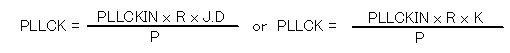
R = 1, 2, 3,4, ... , 15, 16
J = 4,5,6, . . . 63, and D = 0000, 0001, 0002, . . . 9999
K = [J value].[D value]
P = 1, 2, 3, ... 15
R, J, D, and P are programmable. J is the integer portion of K (the numbers to the left of the decimal point), while D is the fractional portion of K (the numbers to the right of the decimal point, assuming four digits of precision).
8.8.5.1 Examples:
- If K = 8.5, then J = 8, D = 5000
- If K = 7.12, then J = 7, D = 1200
- If K = 14.03, then J = 14, D = 0300
- If K = 6.0004, then J = 6, D = 0004
When the PLL is enabled and D = 0000, the following conditions must be satisfied:
- 1MHz ≤ ( PLLCKIN / P ) ≤ 20MHz
- 64MHz ≤ (PLLCKIN x K x R / P ) ≤ 100MHz (in VREF mode)
- 72MHz ≤ (PLLCKIN x K x R / P ) ≤ 86MHz (in VCOM mode)
- 1 ≤ J ≤ 63
When the PLL is enabled and D ≠ 0000, the following conditions must be satisfied:
- 6.667MHz ≤ PLLCLKIN / P ≤ 20MHz
- 64MHz ≤ (PLLCKIN x K x R / P ) ≤ 100MHz (in VREF mode)
- 72MHz ≤ (PLLCK IN x K x R / P ) ≤ 86MHz (in VCOM mode)
- 4 ≤ J ≤ 11
- R = 1
When the PLL is enabled,
- fS = (PLLCLKIN × K × R) / (2048 × P)
- The value of N is selected so that fS × N = PLLCLKIN x K x R / P is in the allowable range.
Example: MCLK = 12MHz and fS = 44.1kHz, (N=2048)
Select P = 1, R = 1, K = 7.5264, which results in J = 7, D = 5264
Example: MCLK = 12MHz and fS = 48.0kHz, (N=2048)
Select P = 1, R = 1, K = 8.192, which results in J = 8, D = 1920
Values are written to the registers in Table 35.
8.8.5.1.1 Recommended PLL settings
Recommended values for the PLL can be found after the register descriptions in this datasheet. Different values are defined based on the device configuration for VREF or VCOM mode.
Other configurations are possible, at your own risk.
Below are details of the register locations, as well as the nomenclature for the table of registers found at the end of this document.
Table 35. PLL Registers
| Divider | Function | Bits |
| PLLE | PLL enable | Page 0, Register 4, D(0) |
| PPDV | PLL P | Page 0, Register 20, D(3:0) |
| PJDV | PLL J | Page 0, Register 21, D(5:0) |
| PDDV | PLL D | Page 0, Register 22, D(5:0) |
| Page 0, Register 23, D(7:0) | ||
| PRDV | PLL R | Page 0, Register 24, D(3:0) |
Table 36. PLL Configuration Recommendations
| Column | Description |
|---|---|
| fS (kHz) | Sampling frequency |
| RSCK | Ratio between sampling frequency and SCK frequency (SCK frequency = RSCK x sampling frequency) |
| SCK (MHz) | System master clock frequency at SCK input (pin 20) |
| PLL VCO (MHz) | PLL VCO frequency as PLLCK in Figure 68 |
| P | One of the PLL coefficients in Equation 3 |
| PLL REF (MHz) | Internal reference clock frequency which is produced by SCK / P |
| M = K * R | The final PLL multiplication factor computed from K and R as described in Equation 3 |
| K = J.D | One of the PLL coefficients in Equation 3 |
| R | One of the PLL coefficients in Equation 3 |
| PLL fS | Ratio between fS and PLL VCO frequency (PLL VCO / fS) |
| DSP fS | Ratio between miniDSP operating clock rate and fS (PLL fS / NMAC) |
| NMAC | The miniDSP clock divider value in Table 34 |
| DSP CLK (MHz) | The miniDSP operating frequency as DSPCK in Figure 68 |
| MOD fS | Ratio between DAC operating clock frequency and fS (PLL fS / NDAC) |
| MOD f (kHz) | DAC operating frequency as DACCK in |
| NDAC | DAC clock divider value in Table 34 |
| DOSR | OSR clock divider value in Table 34 for generating OSRCK in Figure 68. DOSR must be chosen so that MOD fS / DOSR = 16 for correct operation. |
| NCP | NCP (negative charge pump) clock divider value in Table 34 |
| CP f | Negative charge pump clock frequency (fS * MOD fS / NCP) |
| % Error | Percentage of error between PLL VCO / PLL fS and fS (mismatch error).
|
8.8.6 Clock Master Mode from Audio Rate Master Clock
In Master Mode, the device generates bit clock (BCK) and left-right clock (LRCK) and outputs them on the appropriate pins. To configure the device in this mode, first put the device into reset, then use registers BCKO and LRKO (Pg 0, Reg 9 0x09). Then reset the LRCK and BCK divider counters using bits RBCK and RLRK (Pg 0, Reg 12 0x0C). Finally exit reset.
An example of this is given in Register Programming Examples SLAC622.
Figure 69 shows a simplified serial port clock tree for the device in master mode.
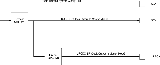 Figure 69. Simplified clock tree for SCK sourced master mode
In master mode, SCK is an input and BCK/LRCK are outputs. BCK and LRCK are integer divisions of SCK. Master mode with a non-audio rate master clock source will require external GPIO’s to use the PLL in standalone mode.
The PLL will also need to be configured to ensure that the onchip miniDSP processor can be driven at its maximum clock rate.
Register changes that need to be done include switching the device into master mode, and setting the divider ratio.
Here is an example of using 24.576MCLK as a master clock source and driving the BCK and LRCK with integer dividers to create 48kHz.
In this mode, the DAC section of the device is also running from the PLL output. While the PLL inside the PCM5242 is one that has been spec’d well enough to achieve the stated performance, using the SCK CMOS Oscillator source will have less jitter.
To switch the DAC clocks (SDAC in the Figure 68) the following registers should be modified
- Clock Tree Flex Mode ( Page 253, Registers 0x3F and 0x40)
- DAC & OSR Source Clock Register (Page 0, Reg 14) – set to 0x30 (SCK input, and OSR is set to whatever the DAC source is)
- The DAC clock divider should be 16FS.
- 16*48kHz = 768kHz
- 24.576MHz (SCK in) / 768kHz = 32
- Therefor, divide ratio for register DDAC (Page 0, Reg 28 0x1C) should be set to 32. The may the register is mapped gives 0x00 = 1, so 32 must be converter to 0x1F (31dec).
An example configuration can be found in SLAC622
8.8.7 Clock Master from a Non-Audio Rate Master Clock
The classic example here is running 12MHz Master clock for a 48kHz sampling system. Given the clock tree for the device (shown in Figure 68), a non-audio clock rate cannot be brought into the SCK to the PLL in master mode. Therefore, the PLL source must be configured to be a GPIO pin, and the output brought back into another GPIO pin.
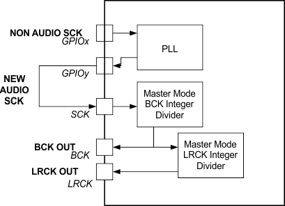 Figure 70. Application diagram for using non-audio clock sources to generate audio clocks
The clock flow through the system is shown above. The newly generated SCK must be brought out of the device on a GPIO pin, then brought into the SCK pin for integer division to create BCK and LRCK outputs.
NOTE
Pull up resistors should be used on BCK and LRCK in this mode to ensure the device doesn't go into sleep mode.
A code example for configuring this mode is provided in SLAC622
8.9 Device Functional Modes
8.9.1 Choosing A Control Mode
SPI Mode is selected by connecting MODE1 to DVDD. SPI mode uses four signal lines and allows higher-speed full-duplex communication between the host and the PCM5242.
I2C Mode is selected by connecting MODE1 to DGND and Mode2 to DVDD. I2C uses two signal lines for half-duplex communication, and is widely used in a variety of devices.
Hardware Control Mode is selected by connecting both MODE1 and MODE2 pins to DGND. Hardware control is useful in applications that do not require on-the-fly device-reconfiguration changes in operating features such as gain or filter latency selection.
See Pin Assignments for a comparison of pin assignments for the 32-terminal QFN.
8.9.1.1 Software Control
8.9.1.1.1 SPI Interface
The SPI interface is a 4-wire synchronous serial port which operates asynchronously to the serial audio interface and the system clock (SCK). The serial control interface is used to program and read the on-chip mode registers.
The control interface includes MISO (pin 24), MOSI (pin 11), MC (pin 12), and MS (pin 18). MISO (Master In Slave Out) is the serial data output, used to read back the values of the mode registers; MOSI (Master Out Slave In) is the serial data input, used to program the mode registers.
MC is the serial bit clock, used to shift data in and out of the control port by falling edge of MC, and MS is the mode control enable with LOW active, used to enable the internal mode register access. If feedback from the device is not required, the MISO pin can be assigned to GPIO1 by register control.
8.9.1.1.1.1 Register Read/Write Operation
All read/write operations for the serial control port use 16-bit data words. Figure 71 shows the control data word format. The most significant bit is the read/write bit. For write operations, the bit must be set to 0. For read operations, the bit must be set to 1. There are seven bits, labeled IDX[6:0], that hold the register index (or address) for the read and write operations. The least significant eight bits, D[7:0], contain the data to be written to, or the data that was read from, the register specified by IDX[6:0].
Figure 71 and Figure 72 show the functional timing diagram to write or read through the serial control port. MS is held at a logic-1 state until a register access. To start the register write or read cycle, set MS to logic 0. Sixteen clocks are then provided on MC, corresponding to the 16 bits of the control data word on MOSI and read-back data on MISO. After the eighth clock cycle has completed, the data from the indexed-mode control register appears on MISO during the read operation. After the sixteenth clock cycle has completed, the data is latched into the indexed-mode control register during the write operation. To write or read subsequent data, MS is set to logic 1 once (See tMHH in Figure 76).
 Figure 71. Control Data Word Format; MDI
NOTE
B8 is used for selection of “Write” or “Read”. Setting = 0 indicates a “Write”, while = 1 indicates a ”Read”. Bits 15–9 are used for register address. Bits 7–0 are used for register data. Multiple-byte write or read (up to 8 bytes) is supported while MS is kept low. The address field becomes the initial address, automatically incrementing for each byte.
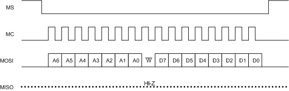 Figure 72. Serial Control Format; Write, Single Byte
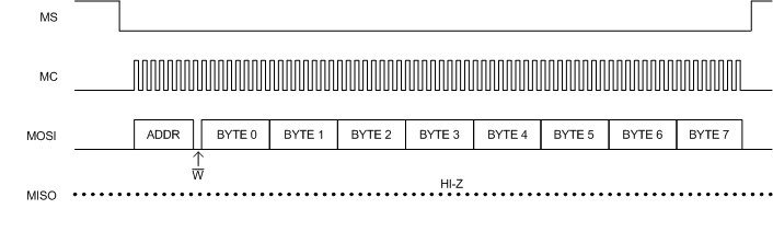 Figure 73. Serial Control Format; Write, Multiple Byte
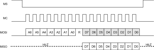 Figure 74. Serial Control Format; Read
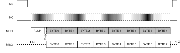 Figure 75. Serial Control Format; Read, Multiple Byte
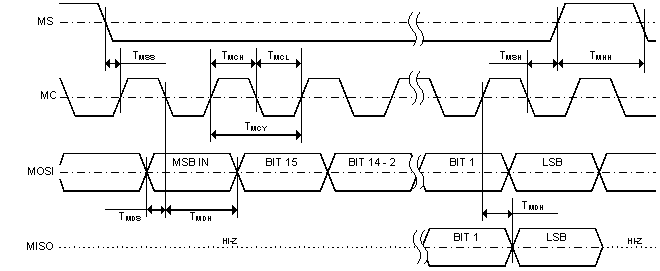 Figure 76. Control Interface Timing
Table 37. Control Interface Timing
| Parameters | Min | Max | Units | |
| tMCY | MC Pulse Cycle Time | 100 | ns | |
| tMCL | MC Low Level Time | 40 | ||
| tMCH | MC High Level Time | 40 | ||
| tMHH | MS High Level Time | 20 | ||
| tMSS | MS ↓ Edge to MC ↑ Edge | 30 | ||
| tMSH | MS Hold Time(1) | 30 | ||
| tMDH | MDI Hold Time | 15 | ||
| tMDS | MDI Set-up Time | 15 | ||
| tMOS | MC Rise Edge to MDO Stable | 20 |
8.9.1.1.2 I2C Interface
The PCM5242 supports the I2C serial bus and the data transmission protocol for standard and fast mode as a slave device.
In I2C mode, the control terminals are changed as follows.
Table 38. I2C Pins and Functions
| Signal | Pin | I/O | Description |
|---|---|---|---|
| SDA | 11 | I/O | I2C data |
| SCL | 12 | I | I2C clock |
| ADR2 | 16 | I | I2C address 2 |
| ADR1 | 24 | I | I2C address 1 |
8.9.1.1.2.1 Slave Address
Table 39. I2C Slave Address
| MSB | LSB | ||||||
| 1 | 0 | 0 | 1 | 1 | ADR2 | ADR1 | R/ W |
The PCM5242 has 7 bits for its own slave address. The first five bits (MSBs) of the slave address are factory preset to 10011 (0x9x). The next two bits of the address byte are the device select bits which can be user-defined by the ADR1 and ADR0 terminals. A maximum of four devices can be connected on the same bus at one time. This gives a range of 0x98, 0x9A, 0x9C and 0x9E. Each PCM5242 responds when it receives its own slave address.
8.9.1.1.2.2 Register Address Auto-Increment Mode
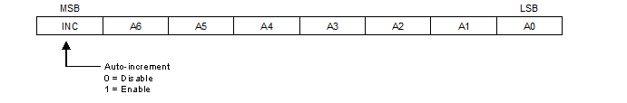 Figure 77. Auto Increment Mode
Auto-increment mode allows multiple sequential register locations to be written to or read back in a single operation, and is especially useful for block write and read operations.
8.9.1.1.2.3 Packet Protocol
A master device must control packet protocol, which consists of start condition, slave address, read/write bit, data if write or acknowledge if read, and stop condition. The PCM5242 supports only slave receivers and slave transmitters.
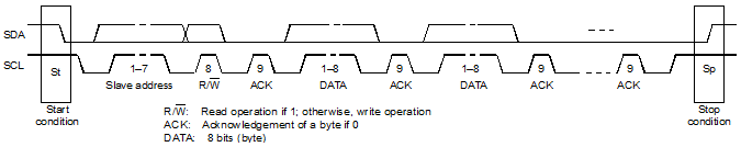 Figure 78. Packet Protocol
Table 40. Write Operation - Basic I2C Framework
| Transmitter | M | M | M | S | M | S | M | S | S | M | |
| Data Type | St | slave address | R/ | ACK | DATA | ACK | DATA | ACK | ACK | Sp |
Table 41. Read Operation - Basic I2C Framework
| Transmitter | M | M | M | S | S | M | S | M | M | M | |
| Data Type | St | slave address | R/ | ACK | DATA | ACK | DATA | ACK | NACK | Sp |
M = Master Device; S = Slave Device; St = Start Condition Sp = Stop Condition
8.9.1.1.2.4 Write Register
A master can write to any PCM5242 registers using single or multiple accesses. The master sends a PCM5242 slave address with a write bit, a register address with auto-increment bit, and the data. If auto-increment is enabled, the address is that of the starting register, followed by the data to be transferred. When the data is received properly, the index register is incremented by 1 automatically. When the index register reaches 0x7F, the next value is 0x0. Table 42 shows the write operation.
Table 42. Write Operation
| Transmitter | M | M | M | S | M | S | M | S | M | S | S | M | ||
| Data Type | St | slave addr | W | ACK | inc | reg addr | ACK | write data 1 | ACK | write data 2 | ACK | ACK | Sp | |
M = Master Device; S = Slave Device; St = Start Condition Sp = Stop Condition; W = Write; ACK = Acknowledge
8.9.1.1.2.5 Read Register
A master can read the PCM5242 register. The value of the register address is stored in an indirect index register in advance. The master sends a PCM5242 slave address with a read bit after storing the register address. Then the PCM5242 transfers the data which the index register points to. When auto-increment is enabled, the index register is incremented by 1 automatically. When the index register reaches 0x7F, the next value is 0x0. Table 43 shows the read operation.
Table 43. Read Operation
| Transmitter | M | M | M | S | M | S | M | M | M | S | S | M | M | M | ||
| Data Type | St | slave addr | W | ACK | inc | reg addr | ACK | Sr | slave addr | R | ACK | data | ACK | NACK | Sp | |
M = Master Device; S = Slave Device; St = Start Condition; Sr = Repeated start condition; Sp = Stop Condition; W = Write; R = Read; NACK = Not acknowledge
8.9.1.1.2.6 Timing Characteristics
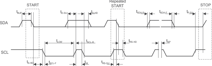 Figure 79. Register Access Timing
Table 44. I2C Bus Timing
| SYMBOL | PARAMETER | CONDITIONS | MIN | MAX | UNIT |
|---|---|---|---|---|---|
| fSCL | SCL clock frequency | Standard | 100 | kHz | |
| Fast | 400 | kHz | |||
| tBUF | Bus free time between a STOP and START condition | Standard | 4.7 | µs | |
| Fast | 1.3 | ||||
| tLOW | Low period of the SCL clock | Standard | 4.7 | µs | |
| Fast | 1.3 | ||||
| tHI | High period of the SCL clock | Standard | 4.0 | µs | |
| Fast | 600 | ns | |||
| tRS-SU | Setup time for (repeated)START condition | Standard | 4.7 | µs | |
| Fast | 600 | ns | |||
| tS-HD | Hold time for (repeated)START condition | Standard | 4.0 | µs | |
| tRS-HD | Fast | 600 | ns | ||
| tD-SU | Data setup time | Standard | 250 | ns | |
| Fast | 100 | ||||
| tD-HD | Data hold time | Standard | 0 | 900 | ns |
| Fast | 0 | 900 | |||
| tSCL-R | Rise time of SCL signal | Standard | 20 + 0.1CB | 1000 | ns |
| Fast | 20 + 0.1CB | 300 | |||
| tSCL-R1 | Rise time of SCL signal after a repeated START condition and after an acknowledge bit | Standard | 20 + 0.1CB | 1000 | ns |
| Fast | 20 + 0.1CB | 300 | |||
| tSCL-F | Fall time of SCL signal | Standard | 20 + 0.1CB | 1000 | ns |
| Fast | 20 + 0.1CB | 300 | |||
| tSDA-R | Rise time of SDA signal | Standard | 20 + 0.1CB | 1000 | ns |
| Fast | 20 + 0.1CB | 300 | |||
| tSDA-F | Fall time of SDA signal | Standard | 20 + 0.1CB | 1000 | ns |
| Fast | 20 + 0.1CB | 300 | |||
| tP-SU | Setup time for STOP condition | Standard | 4.0 | µs | |
| Fast | 600 | ns | |||
| CB | Capacitive load for SDA and SCL line | 400 | pF | ||
| tSP | Pulse width of spike suppressed | Fast | 50 | ns | |
| VNH | Noise margin at High level for each connected device (including hysteresis) | 0.2VDD | V |
8.9.2 Choosing Between VREF and VCOM Modes
See Choosing Between VREF and VCOM Modes for information on configuring these modes.