SLASE63 November 2014 PCM5252
PRODUCTION DATA.
- 1 Features
- 2 Applications
- 3 Description
- 4 Revision History
- 5 Device Comparison
- 6 Pin Configuration and Functions
-
7 Specifications
- 7.1 Absolute Maximum Ratings
- 7.2 ESD Ratings
- 7.3 Recommended Operating Conditions
- 7.4 Thermal Information
- 7.5 Electrical Characteristics
- 7.6 Switching Characteristics
- 7.7 Timing Requirements: SCK Input
- 7.8 Timing Requirements: PCM Audio Data
- 7.9 Timing Requirements: I2S Master, See
- 7.10 Timing Requirements: XSMT
- 7.11 Typical Characteristics
-
8 Detailed Description
- 8.1 Overview
- 8.2 Functional Block Diagram
- 8.3
Feature Description
- 8.3.1 Terminology
- 8.3.2 Audio Data Interface
- 8.3.3 XSMT Pin (Soft Mute / Soft Un-Mute)
- 8.3.4 Audio Processing
- 8.3.5 DAC and Differential Analog Outputs
- 8.3.6
Reset and System Clock Functions
- 8.3.6.1 Clocking Overview
- 8.3.6.2 Clock Slave Mode With Master and System Clock (SCK) Input (4 Wire I2S)
- 8.3.6.3 Clock Slave Mode With BCK PLL to Generate Internal Clocks (3-Wire PCM)
- 8.3.6.4 Clock Generation Using the PLL
- 8.3.6.5 PLL Calculation
- 8.3.6.6 Clock Master Mode from Audio Rate Master Clock
- 8.3.6.7 Clock Master from a Non-Audio Rate Master Clock
- 8.4 Device Functional Modes
- 9 Application and Implementation
-
10Power Supply Recommendations
- 10.1 Power Supply Distribution and Requirements
- 10.2 Recommended Powerdown Sequence
- 10.3 External Power Sense Undervoltage Protection Mode
- 10.4 Power-On Reset Function
- 10.5 PCM5252 Power Modes
-
11Layout
- 11.1
Layout Guidelines
- 13.2.1.2.19 Page 0 / Register 24
- 13.2.1.2.20 Page 0 / Register 27
- 13.2.1.2.21 Page 0 / Register 28
- 13.2.1.2.22 Page 0 / Register 29
- 13.2.1.2.23 Page 0 / Register 30
- 13.2.1.2.24 Page 0 / Register 32
- 13.2.1.2.25 Page 0 / Register 33
- 13.2.1.2.26 Page 0 / Register 34
- 13.2.1.2.27 Page 0 / Register 35
- 13.2.1.2.28 Page 0 / Register 36
- 13.2.1.2.29 Page 0 / Register 37
- 13.2.1.2.30 Page 0 / Register 40
- 13.2.1.2.31 Page 0 / Register 41
- 13.2.1.2.32 Page 0 / Register 42
- 13.2.1.2.33 Page 0 / Register 43
- 13.2.1.2.34 Page 0 / Register 44
- 13.2.1.2.35 Page 0 / Register 59
- 13.2.1.2.36 Page 0 / Register 60
- 13.2.1.2.37 Page 0 / Register 61
- 13.2.1.2.38 Page 0 / Register 62
- 13.2.1.2.39 Page 0 / Register 63
- 13.2.1.2.40 Page 0 / Register 64
- 13.2.1.2.41 Page 0 / Register 65
- 13.2.1.2.42 Page 0 / Register 80
- 13.2.1.2.43 Page 0 / Register 81
- 13.2.1.2.44 Page 0 / Register 82
- 13.2.1.2.45 Page 0 / Register 83
- 13.2.1.2.46 Page 0 / Register 84
- 13.2.1.2.47 Page 0 / Register 85
- 13.2.1.2.48 Page 0 / Register 86
- 13.2.1.2.49 Page 0 / Register 87
- 13.2.1.2.50 Page 0 / Register 90
- 13.2.1.2.51 Page 0 / Register 91
- 13.2.1.2.52 Page 0 / Register 92
- 13.2.1.2.53 Page 0 / Register 93
- 13.2.1.2.54 Page 0 / Register 94
- 13.2.1.2.55 Page 0 / Register 95
- 13.2.1.2.56 Page 0 / Register 108
- 13.2.1.2.57 Page 0 / Register 109
- 13.2.1.2.58 Page 0 / Register 114
- 13.2.1.2.59 Page 0 / Register 115
- 13.2.1.2.60 Page 0 / Register 118
- 13.2.1.2.61 Page 0 / Register 119
- 13.2.1.2.62 Page 0 / Register 120
- 13.2.1.2.63 Page 0 / Register 121
- 13.2.1.2.64 Page 0 / Register 122
- 13.2.1.2.65 Page 0 / Register 123
- 13.2.1.2.66 Page 0 / Register 124
- 13.2.1.2.67 Page 0 / Register 125
- 11.2 Layout Example
- 11.1
Layout Guidelines
- 12Programming
- 13Register Maps
- 14Device and Documentation Support
- 15Mechanical, Packaging, and Orderable Information
- 14Device and Documentation Support
- 15Mechanical, Packaging, and Orderable Information
7 Specifications
7.1 Absolute Maximum Ratings
over operating free-air temperature range (unless otherwise noted)| MIN | MAX | UNIT | ||
|---|---|---|---|---|
| Supply voltage | AVDD, CPVDD, DVDD | –0.3 | 3.9 | V |
| LDO with DVDD at 1.8 V | –0.3 | 2.25 | ||
| Digital input voltage | DVDD at 1.8 V | –0.3 | 2.25 | V |
| DVDD at 3.3 V | –0.3 | 3.9 | ||
| Analog input voltage | –0.3 | 3.9 | V | |
| Storage temperature, Tstg | –40 | 125 | °C | |
7.2 ESD Ratings
| VALUE | UNIT | |||
|---|---|---|---|---|
| V(ESD) | Electrostatic discharge | Human-body model (HBM), per ANSI/ESDA/JEDEC JS-001(1) | ±2500 | V |
| Charged-device model (CDM), per JEDEC specification JESD22-C101(2) | ±1500 | |||
(1) JEDEC document JEP155 states that 500-V HBM allows safe manufacturing with a standard ESD control process.
(2) JEDEC document JEP157 states that 250-V CDM allows safe manufacturing with a standard ESD control process.
7.3 Recommended Operating Conditions
| MIN | NOM | MAX | UNIT | ||||
|---|---|---|---|---|---|---|---|
| AVDD | Analog power supply voltage | Referenced to AGND(1) | VCOM mode | 3 | 3.3 | 3.46 | V |
| VREF mode | 3.2 | 3.3 | 3.46 | ||||
| DVDD | Digital power supply voltage | Referenced to DGND(1) | 1.8 V DVDD | 1.65 | 1.8 | 1.95 | V |
| 3.3 V DVDD | 3.1 | 3.3 | 3.46 | ||||
| CPVDD | Charge pump supply voltage | Referenced to CPGND(1) | 3.1 | 3.3 | 3.46 | V | |
| MCLK | Master clock frequency | 50 | MHz | ||||
| LOL, LOR | Stereo line output load resistance | 2 | 10 | kΩ | |||
| CLOUT | Digital output load capacitance | 10 | pF | ||||
| TJ | Operating junction temperature | –25 | 85 | °C | |||
(1) All grounds on board are tied together; they must not differ in voltage by more than 0.2-V maximum, for any combination of ground signals.
7.4 Thermal Information
| THERMAL METRIC(1) | PW | UNIT | |
|---|---|---|---|
| 20 PINS | |||
| RθJA | Junction-to-ambient thermal resistance | 91.2 | °C/W |
| RθJC(top) | Junction-to-case (top) thermal resistance | 25.3 | °C/W |
| RθJB | Junction-to-board thermal resistance | 42 | °C/W |
| ψJT | Junction-to-top characterization parameter | 1 | °C/W |
| ψJB | Junction-to-board characterization parameter | 41.5 | °C/W |
| RθJC(bot) | Junction-to-case (bottom) thermal resistance | — | °C/W |
(1) For more information about traditional and new thermal metrics, see the Semiconductor and IC Package Thermal Metrics application report.
7.5 Electrical Characteristics
All specifications at TA = 25°C, AVDD = CPVDD = DVDD = 3.3V, fS = 48kHz, system clock = 512 fS and 24-bit data unless otherwise noted.| PARAMETER | TEST CONDITIONS | MIN | TYP | MAX | UNIT | ||
|---|---|---|---|---|---|---|---|
| Resolution | 16 | 24 | 32 | Bits | |||
| Digital Input/Output | |||||||
| Logic family: 3.3 V LVCMOS compatible | |||||||
| VIH | Input logic level, high | 0.7×DVDD | V | ||||
| VIL | Input logic level, low | 0.3×DVDD | V | ||||
| IIH | Input logic current, high | VIN = VDD | 10 | µA | |||
| IIL | Input logic current, low | VIN = 0 V | –10 | µA | |||
| VOH | Output logic level, high | IOH = –4 mA | 0.8×DVDD | V | |||
| VOL | Output logic level, low | IOL = 4 mA | 0.22×DVDD | V | |||
| Logic family 1.8 V LVCMOS compatible | |||||||
| VIH | Input logic level, high | 0.7×DVDD | V | ||||
| VIL | Input logic level, low | 0.3×DVDD | V | ||||
| IIH | Input logic current, high | VIN = VDD | 10 | µA | |||
| IIL | Input logic current, low | VIN = 0 V | –10 | µA | |||
| VOH | Output logic level, high | IOH = –2 mA | 0.8×DVDD | V | |||
| VOL | Output logic level, low | IOL = 2 mA | 0.22×DVDD | V | |||
| Dynamic Performance (PCM Mode)(1)(2) | |||||||
| THD+N at –1 dBFS(2) | fS = 48 kHz | –93 | –83 | dB | |||
| fS = 96 kHz | –93 | ||||||
| fS = 192 kHz | –93 | ||||||
| Dynamic range(2) | EIAJ, A-weighted, fS = 48 kHz | 108 | 114 | dB | |||
| EIAJ, A-weighted, fS = 96 kHz | 114 | ||||||
| EIAJ, A-weighted, fS = 192 kHz | 114 | ||||||
| Signal-to-noise ratio(2) | EIAJ, A-weighted, fS = 48 kHz | 114 | dB | ||||
| EIAJ, A-weighted, fS = 96 kHz | 114 | ||||||
| EIAJ, A-weighted, fS = 192 kHz | 114 | ||||||
| Signal to noise ratio with analog mute(2)(3) | EIAJ, A-weighted, fS = 48 kHz | 113 | 123 | dB | |||
| EIAJ, A-weighted, fS = 96 kHz | 113 | 123 | |||||
| EIAJ, A-weighted, fS = 192 kHz | 113 | 123 | |||||
| Channel separation | fS = 48 kHz | 100 / 95 | 109 / 103 | dB | |||
| fS = 96 kHz | 100 / 95 | 109 / 103 | |||||
| fS = 192 kHz | 100 / 95 | 109 / 103 | |||||
| Analog Output | |||||||
| Single Ended Output voltage | 2.1 | VRMS | |||||
| Differential Output Voltage | 4.2 | VRMS | |||||
| Gain error | –6 | ±2 | 6 | % of FSR | |||
| Gain mismatch, channel-to-channel | –6 | ±2 | 6 | % of FSR | |||
| Bipolar zero error (per pin) | At bipolar zero | –2 | ±1 | 2 | mV | ||
| Load impedance | 5 | kΩ | |||||
| Filter Characteristics–1: Normal (8x) | |||||||
| Pass band | 0.45fS | ||||||
| Stop band | 0.55fS | ||||||
| Stop band attenuation | –60 | dB | |||||
| Pass-band ripple | ±0.02 | dB | |||||
| Delay time | 20fS | s | |||||
| Filter Characteristics–2: Low Latency (8x) | |||||||
| Pass band | 0.47fS | ||||||
| Stop band | 0.55fS | ||||||
| Stop band attenuation | –52 | dB | |||||
| Pass-band ripple | ±0.0001 | dB | |||||
| Delay time | 3.5fS | s | |||||
| Filter Characteristics–3: Asymmetric FIR (8x) | |||||||
| Pass band | 0.40fS | ||||||
| Stop band | 0.72fS | ||||||
| Stop band attenuation | –52 | dB | |||||
| Pass-band ripple | ±0.05 | dB | |||||
| Delay time | 1.2fS | s | |||||
| Filter Characteristics–4: High-Attenuation (8x) | |||||||
| Pass band | 0.45fS | ||||||
| Stop band | 0.45S | ||||||
| Stop band attenuation | –100 | dB | |||||
| Pass-band ripple | ±0.0005 | dB | |||||
| Delay time | 33.7fS | s | |||||
| Power Supply Requirements | |||||||
| DVDD | Digital supply voltage | Target DVDD = 1.8 V | 1.65 | 1.8 | 1.95 | VDC | |
| DVDD | Digital supply voltage | Target DVDD = 3.3 V | 3 | 3.3 | 3.6 | VDC | |
| AVDD | Analog supply voltage | 3 | 3.3 | 3.6 | VDC | ||
| CPVDD | Charge-pump supply voltage | 3 | 3.3 | 3.6 | VDC | ||
| IDD | DVDD supply current at 1.8 V | fS = 48 kHz, Input is Bipolar Zero data | 11 | 14 | mA | ||
| fS = 96 kHz, Input is Bipolar Zero data | 12 | ||||||
| fS = 192 kHz, Input is Bipolar Zero data | 14 | ||||||
| IDD | DVDD supply current at 1.8 V | fS = 48 kHz, Input is 1kHz -1dBFS data | 11 | 14 | mA | ||
| fS = 96 kHz, Input is 1kHz -1dBFS data | 12 | ||||||
| fS = 192 kHz, Input is 1kHz -1dBFS data | 14 | ||||||
| IDD | DVDD supply current at 1.8 V(4) | fS = N/A, Power Down Mode | 0.3 | 0.6 | mA | ||
| IDD | DVDD supply current at 3.3 V | fS = 48 kHz, Input is Bipolar Zero data | 12 | 15 | mA | ||
| fS = 96 kHz, Input is Bipolar Zero data | 13 | ||||||
| fS = 192 kHz, Input is Bipolar Zero data | 15 | ||||||
| IDD | DVDD supply current at 3.3 V | fS = 48 kHz, Input is 1kHz -1dBFS data | 12 | 15 | mA | ||
| fS = 96 kHz, Input is 1kHz -1dBFS data | 13 | ||||||
| fS = 192 kHz, Input is 1kHz -1dBFS data | 15 | ||||||
| IDD | DVDD supply current at 3.3 V(4) | fS = N/A, Power Down Mode | 0.5 | 0.8 | mA | ||
| ICC | AVDD / CPVDD supply current | fS = 48 kHz, Input is Bipolar Zero data | 11 | 16 | mA | ||
| fS = 96 kHz, Input is Bipolar Zero data | 11 | ||||||
| fS = 192 kHz, Input is Bipolar Zero data | 11 | ||||||
| ICC | AVDD / CPVDD supply current | fS = 48 kHz, Input is 1kHz -1dBFS data | 24 | 32 | mA | ||
| fS = 96 kHz, Input is 1kHz -1dBFS data | 24 | ||||||
| fS = 192 kHz, Input is 1kHz -1dBFS data | 24 | ||||||
| ICC | AVDD / CPVDD supply current(4) | fS = N/A, Power Down Mode | 0.2 | 0.4 | mA | ||
| Power dissipation, DVDD = 1.8 V | fS = 48 kHz, Input is Bipolar Zero data | 59.4 | 78 | mW | |||
| fS = 96 kHz, Input is Bipolar Zero data | 61.2 | ||||||
| fS = 192 kHz, Input is Bipolar Zero data | 64.8 | ||||||
| Power dissipation, DVDD = 1.8 V | fS = 48 kHz, Input is 1kHz -1dBFS data | 99 | 130.8 | mW | |||
| fS = 96 kHz, Input is 1kHz -1dBFS data | 100.8 | ||||||
| fS = 192 kHz, Input is 1kHz -1dBFS data | 104.4 | ||||||
| Power dissipation, DVDD = 1.8 V(4) | fS = N/A (Power Down Mode) | 1.2 | mW | ||||
| Power dissipation, DVDD = 3.3 V | fS = 48 kHz, Input is Bipolar Zero data | 79.2 | 103 | mW | |||
| fS = 96 kHz, Input is Bipolar Zero data | 82.5 | ||||||
| fS = 192 kHz, Input is Bipolar Zero data | 89.1 | ||||||
| Power dissipation, DVDD = 3.3 V | fS = 48 kHz, Input is 1kHz -1dBFS data | 118.8 | 155 | mW | |||
| fS = 96 kHz, Input is 1kHz -1dBFS data | 122.1 | ||||||
| fS = 192 kHz, Input is 1kHz -1dBFS data | 128.7 | ||||||
| Power dissipation, DVDD = 3.3 V(4) | fS = N/A (Power Down Mode) | 2.3 | 4 | mW | |||
(1) Filter condition: THD+N: 20-Hz HPF, 20-kHz AES17 LPF; Dynamic range: 20-Hz HPF, 20-kHz AES17 LPF; A-weighted signal-to-noise ratio: 20-Hz HPF, 20-kHz AES17 LPF; A-weighted channel separation: 20-Hz HPF, 20-kHz AES17 LPF. Analog performance specifications are measured using the System Two Cascade™ audio measurement system by Audio Precision™ in the RMS mode.
(2) Output load is 10 kΩ, with 470-Ω output resistor and a 2.2-nF shunt capacitor (see recommended output filter).
(3) Assert XSMT or both L-ch and R-ch PCM data are Bipolar Zero.
(4) Power Down Mode, with LRCK, BCK, and SCK halted at Low level.
7.6 Switching Characteristics
over operating free-air temperature range (unless otherwise noted)| PARAMETER | TEST CONDITIONS | MIN | TYP | MAX | UNIT | |
|---|---|---|---|---|---|---|
| DATA FORMAT (PCM MODE) | ||||||
| Audio data interface format | I2S, left-justified, right-justified, and TDM | |||||
| Audio data bit length | 16, 20, 24, 32-bit acceptable | |||||
| Audio data format | MSB first, twos-complement | |||||
| fS | Sampling frequency(1) | 8 | 384 | kHz | ||
| CLOCKS | ||||||
| System clock frequency | 64, 128, 192, 256, 384, 512, 768, 1024, 1152, 1536, 2048, or 3072 fSCK, up to 50 Mhz |
|||||
| PLL input frequency (2) | Clock divider uses fractional divide D > 0, P=1 |
6.7 | 20 | MHz | ||
| Clock divider uses integer divide D = 0, P=1 |
1 | 20 | MHz | |||
(1) One sample time is defined as the reciprocal of the sampling frequency. 1 × tS = 1 / fS
(2) With the appropriate P coefficient setting, the PLL accepts up to 50 MHz. This clock is then divided to meet the ≤ 20-MHz requirement. See PLL Calculation.
7.7 Timing Requirements: SCK Input
Figure 4 shows the timing requirements for the system clock input. For optimal performance, use a clock source with low phase jitter and noise.| MIN | NOM | MAX | UNIT | |||
|---|---|---|---|---|---|---|
| tSCY | System clock pulse cycle time | 20 | 1000 | ns | ||
| tSCKH | System clock pulse width, high | DVDD = 1.8 V | 8 | ns | ||
| DVDD = 3.3 V | 9 | |||||
| tSCKL | System clock pulse width, low | DVDD = 1.8 V | 8 | ns | ||
| DVDD = 3.3 V | 9 | |||||
 Figure 4. Timing Requirements for SCK Input
7.8 Timing Requirements: PCM Audio Data
| MIN | NOM | MAX | UNIT | ||
|---|---|---|---|---|---|
| tBCY | BCK Pulse Cycle Time | 40 | ns | ||
| tBCL | BCK Pulse Width LOW | 16 | ns | ||
| tBCH | BCK Pulse Width HIGH | 16 | ns | ||
| tBL | BCK Rising Edge to LRCK Edge | 8 | ns | ||
| tBCK | BCK frequency at DVDD = 3.3V | 24.576 | MHz | ||
| tBCK(1.8V) | BCK frequency at DVDD = 1.8V | 12.288 | MHz | ||
| tLB | LRCK Edge to BCK Rising Edge | 8 | ns | ||
| tDS | DATA Set Up Time | 8 | ns | ||
| tDH | DATA Hold Time | 8 | ns | ||
| tDOD | DATA delay time from BCK falling edge | 15 | ns | ||
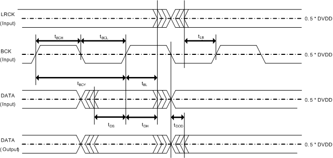 Figure 5. PCM5252 Serial Audio Timing - Slave
In software mode, The PCM5252 can act as an I2S master, generating BCK and LRCK as outputs from the SCK input.
Table 3. I2S Master Mode Registers
| Register | Function |
|---|---|
| Page0, Register 9, D(0), D(4), and D(5) | I2S Master mode select |
| Register 32, D(6:0) | |
| Register 33, D(7:0) | BCK divider and LRCK divider |
7.9 Timing Requirements: I2S Master, See Figure 6
| MIN | NOM | MAX | UNIT | ||
|---|---|---|---|---|---|
| tBCY | BCK Pulse Cycle Time | 40 | ns | ||
| tBCL | BCK Pulse Width LOW | 16 | ns | ||
| tBCH | BCK Pulse Width HIGH | 16 | ns | ||
| tBCK | BCK frequency at DVDD = 3.3 V | 24.576 | MHz | ||
| tBCK(1.8V) | BCK frequency at DVDD = 1.8 V | 12.288 | MHz | ||
| tLRD | LRCKx delay time from BCKx falling edge | –10 | 20 | ns | |
| tDS | DATA Set Up Time | 8 | ns | ||
| tDH | DATA Hold Time | 8 | ns | ||
| tDOD | DATA delay time from BCK falling edge at DVDD = 3.3 V | 15 | ns | ||
| tDOD(1.8V) | DATA delay time from BCK falling edge at DVDD = 1.8 V | 20 | ns | ||
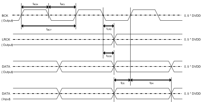 Figure 6. PCM5252 Serial Audio Timing - I2S Master
7.10 Timing Requirements: XSMT
| MIN | NOM | MAX | UNIT | ||
|---|---|---|---|---|---|
| tr | Rise time | 20 | ns | ||
| tf | Fall time | 20 | ns | ||
 Figure 7. XSMT Timing for Soft Mute and Soft Un-Mute
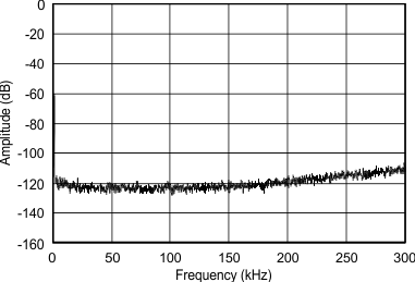
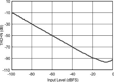
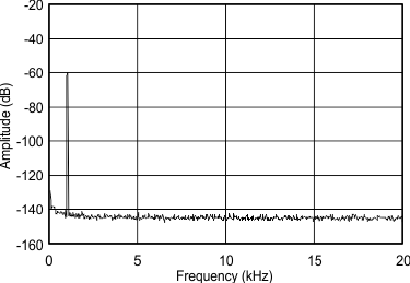
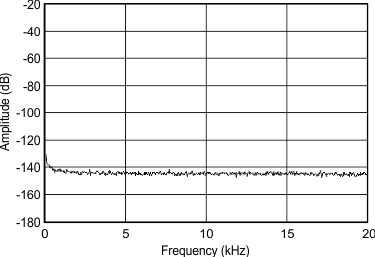
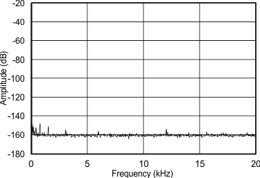
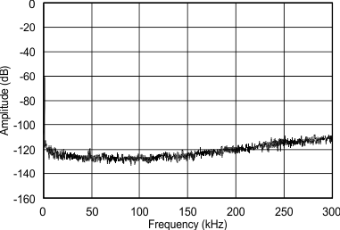
7.11 Typical Characteristics
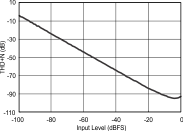
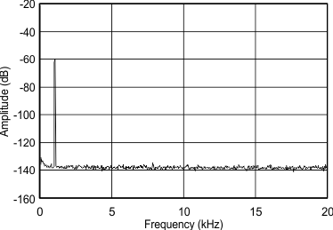
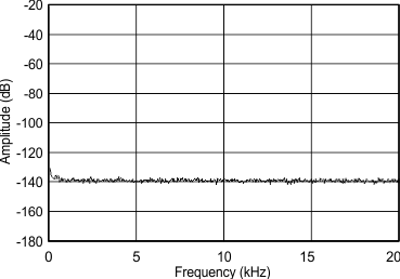
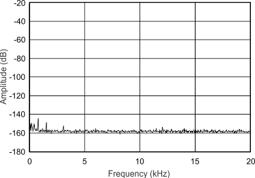
All specifications at TA = 25°C, AVDD = CPVDD = DVDD = 3.3V, fS = 48kHz, system clock = 512 fS and 24-bit data unless otherwise noted.