JAJSFP5E July   2018  – February 2022 REF2025 , REF2030 , REF2033 , REF2041

PRODUCTION DATA  

  1. 特長
  2. アプリケーション
  3. 概要
  4. Revision History
  5. Device Comparison Table
  6. Pin Configuration and Functions
    1.     Pin Functions
  7. Specifications
    1. 7.1 Absolute Maximum Ratings
    2. 7.2 ESD Ratings
    3. 7.3 Recommended Operating Conditions
    4. 7.4 Thermal Information
    5. 7.5 Electrical Characteristics
    6. 7.6 Typical Characteristics
  8. Parameter Measurement Information
    1. 8.1 Solder Heat Shift
    2. 8.2 Long-Term Stability
    3. 8.3 Thermal Hysteresis
    4. 8.4 Noise Performance
  9. Detailed Description
    1. 9.1 Overview
    2. 9.2 Functional Block Diagram
    3. 9.3 Feature Description
      1. 9.3.1 VREF and VBIAS Tracking
      2. 9.3.2 Low Temperature Drift
      3. 9.3.3 Load Current
    4. 9.4 Device Functional Modes
  10. 10Applications and Implementation
    1. 10.1 Application Information
    2. 10.2 Typical Application
      1. 10.2.1 Low-Side, Current-Sensing Application
        1. 10.2.1.1 Design Requirements
        2. 10.2.1.2 Detailed Design Procedure
          1. 10.2.1.2.1 Shunt Resistor
          2. 10.2.1.2.2 Differential Amplifier
          3. 10.2.1.2.3 Voltage Reference
          4. 10.2.1.2.4 Results
        3. 10.2.1.3 Application Curves
  11. 11Power-Supply Recommendations
  12. 12Layout
    1. 12.1 Layout Guidelines
    2. 12.2 Layout Example
  13. 13Device and Documentation Support
    1. 13.1 Documentation Support
      1. 13.1.1 Related Documentation
    2. 13.2 Receiving Notification of Documentation Updates
    3. 13.3 サポート・リソース
    4. 13.4 Trademarks
    5. 13.5 Electrostatic Discharge Caution
    6. 13.6 Glossary
  14. 14Mechanical, Packaging, and Orderable Information

パッケージ・オプション

メカニカル・データ(パッケージ|ピン)
サーマルパッド・メカニカル・データ
発注情報
Shunt Resistor

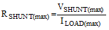
As illustrated in Figure 10-2, the value of VSHUNT is the ground potential for the system load. If the value of VSHUNT is too large, issues may arise when interfacing with systems whose ground potential is actually 0 V. Also, a value of VSHUNT that is too negative may violate the input common-mode voltage of the differential amplifier in addition to potential interfacing issues. Therefore, limiting the voltage across the shunt resistor is important. Equation 6 can be used to calculate the maximum value of RSHUNT.

Equation 6. GUID-0E70FB1E-ED82-48BE-9D98-F0274292C52A-low.gif

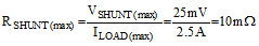
Given that the maximum shunt voltage is ±25 mV and the load current range is ±2.5 A, the maximum shunt resistance is calculated as shown in Equation 7.

Equation 7. GUID-D31E89FE-2DA0-4049-8184-D44E39B77657-low.gif

To minimize errors over temperature, select a low-drift shunt resistor. To minimize offset error, select a shunt resistor with the lowest tolerance. For this design, the Y14870R01000B9W resistor is used.